


News: Optoelectronics
27 April 2023
InAs quantum dot lasers butt-coupled to SOI waveguides
Researchers based in China claim the first demonstration of indium arsenide (InAs) quantum dot lasers epitaxially grown on trenched silicon-on-insulator (SOI) templates with butt-coupled silicon (Si) waveguides (WGs). [Wen-Qi Wei et al. Light: Science & Applications, v12, p84, 2023].
The team from Institute of Physics, Songshan Lake Materials Laboratory, Shanghai Jiao Tong University, and University of Chinese Academy of Sciences, comments: “Our results demonstrate that monolithic integration of III-V laser with silicon photonic components will no longer be a design-level hypothesis.”
Efficient integration of a laser structure with low-cost silicon photonics is highly desirable for a wide range of advanced applications for on-chip optical interconnect and communications, along with integrated optical ranging, for system deployment in artificial intelligence, hyper-scale data centers, high-performance computing, light-detection and ranging (LIDAR) and microwave photonics.
The SOI wafer consisted of 220nm silicon on 3μm buried silicon dioxide (SiO2). The wafer was patterned with a series of silicon waveguides with fork-shaped couplings to improve light energy transfer between the lasers and waveguides. The structures were covered with 3μm plasma-enhanced chemical vapor deposition (PECVD) SiO2 top cladding. A series of 16mmx16mm trenches for the lasers were then etched through to the substrate silicon with a 16% fill factor. The base of the lasers was also patterned with a grating.
The laser structures themselves were grown (Figure 1) using a dual-chamber solid-source molecular beam-epitaxy (MBE) system to enable controlled growth of both silicon (group IV of the periodic table) and III-V materials.
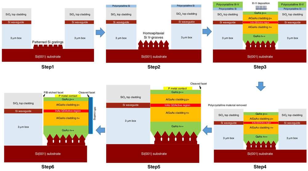
Figure 1: Schematic diagram of embedded laser process on trenched SOI.
The silicon growth created V-groove structures with (111) crystal facets on which the aluminium gallium arsenide (AlGaAs) III-V materials could be grown (Figure 2), avoiding defects such as anti-phase domains (APDs), threading dislocations (TDDs), and thermal-mismatch-induced thermal cracks. Further measures to reduce the effect of defects were applied in the buffer layer growth by including quantum well dislocation filters (DLFs) and superlattice (SL) layers.
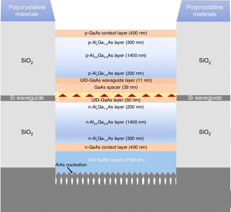
Figure 2: Schematic of the laser epi-structures
After the MBE growth processes, the poly-crystalline residues outside the laser trench were removed with wet etching to enable accurate laser–waveguide alignment. The poly removal also partially etched the laser output facet, whose formation was completed with focused ion-beam (FIB) milling in two steps to give a very smooth surface. The coupling gap between the facets and waveguides was about 5μm.
The back facet was formed by wafer cleaving and application of a 95% high-reflection (HR) coating, consisting of 8 pairs of 145nm/228nm SiO2/niobium pentoxide (Nb2O5) layers.
Photoluminescence experiments on the structure gave an O-band emission peak with 33nm full-width at half-maximum (FWHM). The researchers report that a similar structure grown on gallium arsenide (GaAs) substrate had a surprisingly wider 42nm FWHM. The peak intensity was “almost the same”. The peak wavelengths for the trench template and GaAs substrate were 1293nm and 1278nm, respectively. The longer wavelength resulted from a 20°C lower growth temperature for the seven InAs quantum dot layer active light-generating region, relative to that for the structure on GaAs substrate.
The material was fabricated into 3mmx3μm ridge lasers. A reference device formed by cleaving the front and back facets achieved continuous wave (CW) lasing up to 95°C (Figure 3). At room temperature, the threshold current was 50mA, and the maximum output power 37mW at 250mA. The slope efficiency was 0.148W/A.
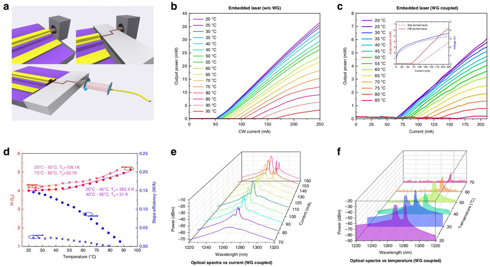
Figure 3: Continuous-wave characterizations of embedded InAs QD laser on SOI with and without coupling into silicon waveguide. a. Measurement schemes. b,c. Light output power versus CW current with and without waveguide coupling. d. Threshold current and slope efficiency versus temperature. e,f. Spectra showing variations against current and temperature.
Lasers coupled to the silicon waveguides had a higher CW threshold current of 65mA, and the maximum operating temperature was reduced to 85°C. The 20°C slope efficiency was 0.025W/A.
The researchers comment: “The relatively higher threshold current and lower maximum operation temperature are attributed to increased thermal accumulation inside the laser trench with surrounding BOX layer.”
One effect of not polishing the output facet with FIB milling was to increase the threshold to 92mA. Also, the out-coupled optical power through the silicon waveguide was reduced to 5.3mW at 210mA, compared with 6.8mW for the FIB-milled lasers at the same injection.
The overall insertion loss of the laser coupling to the waveguide is estimated at -7.35dB, including 0.3dB from two 90° bends in, and 0.62dB from attenuation over the 814μm length of the waveguide. For pulse-mode operation, the loss was –7.6dB.
The characteristic temperature for the increase in threshold current (T0) of the reference device was 282K in the 20–40°C range, and 51K in the 45–95°C range. Coupled to the waveguides, T0 reduced to 108K and 34K for 20–65°C and 70–85°C, respectively.
InAs quantum dot lasers InAs AlGaAs LIDAR MBE SOI waveguides
The author Mike Cooke is a freelance technology journalist who has worked in the semiconductor and advanced technology sectors since 1997.


