


News: LEDs
21 April 2023
Red InGaN LEDs for visible light communication
Fudan University and Jiangxi Latticepower Semiconductor Corp in China claim the first report of red-emission micro-sized light-emitting diodes (micro-LEDs) on silicon substrates for visible light communication [Xinyi Lu et al, Journal of Lightwave Technology, published online 27 March 2023]. The team also studied the wavelength/color shifts from red to green with increased current for various sizes of micro-LED with a view to displays and multi-wavelength data transmission.
The researchers see potential deployment in multi-color displays and high-speed visible light communication, especially for wearable products. Of course, the use in displays would require careful management of pulsed operation to compensate the lower light output power at low current injection relative to high current injection.
The wavelength/color shifts to the bluer part of the visible spectrum arise from effects that are not desired in other application contexts such as band-filling and the quantum-confined Stark effect (QCSE). Band-filling refers to the filling of energy levels as the current injection increases, creating a larger energy drop for electrons recombining into holes. The QCSE arises from electric fields due to charge polarization of the chemical bonds in III-nitride materials, which arise both spontaneously and from piezoelectric strain effects in heterostructures.
The researchers used metal-organic chemical vapor deposition on silicon (111) substrates to grow the indium gallium nitride (InGaN) epitaxial material for the red LEDs (Figure 1). The active region consisted of three InGaN quantum wells (QWs) targeting red emissions.
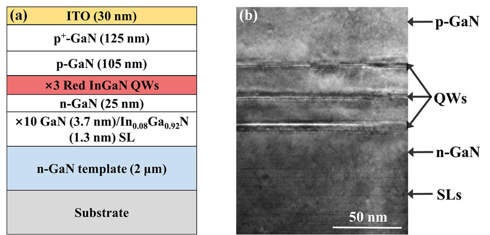
Figure 1: (a) Schematic diagram and (b) cross-sectional transmission electron microscope (TEM) images of InGaN-based red LED epitaxial structure.
Square-pixel LEDs were fabricated with sides varying between 20μm and 150μm. The researchers classified the 150μm device as a ‘mini-LED’, and the smaller ones as ‘micro-LEDs’.
The fabrication began with deposition of a 30nm transparent conducting layer, consisting of indium tin oxide (ITO), for current spreading from the p-electrode. The device mesas were formed by inductively coupled plasma reactive ion etching (ICP-RIE). A 300nm plasma-enhance chemical vapor deposition (PECVD) of silicon dioxide was used for passivation. The n- and p-electrodes were titanium/gold.
Although the series resistance of the smaller devices was higher, due to the smaller cross-sectional area, the forward voltage for 10A/cm2 injection current density was lower: 3.24V for the 20μm micro-LED, compared with 3.84V for the 150μm mini-LED. In other words, the smaller devices have higher conductivity.
The smallest 20μm LED suffered from high leakage current under reverse bias, attributed to sidewall defects acting as current leakage channels. In numbers, the leakage for the 20μm LED was 2.7x10⁻⁵A/cm2 at 5V reverse bias, compared with 2.44x10⁻⁶A/cm2 for the 150μm LED.
Increasing the current injection shifted the peak electroluminescence (EL) wavelength in the shorter-wavelength blue direction, due to screening of the piezoelectric fields, and band-filling, spanning the range 670nm (red) down to 520nm (green) for the 20μm LED (Figure 2).
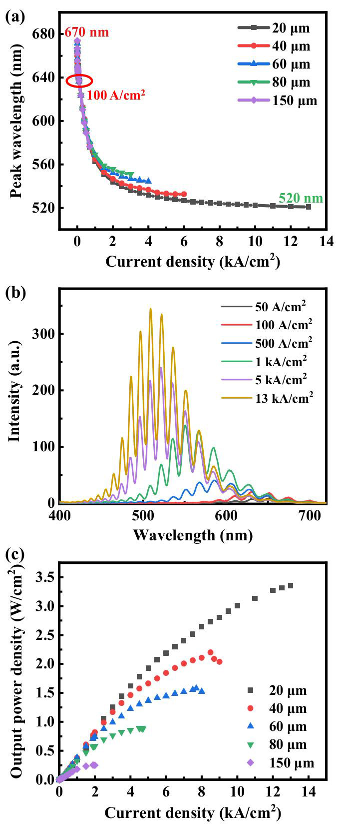
Figure 2: (a) EL peak wavelength versus current density for all chip sizes. (b) EL spectra of 20μm pixel from 50A/cm2 to 13,000A/cm2. (c) Light output power density versus injection current density for all chip sizes.
The combination of silicon substrate and small pixel size enabled the 20μm LED to reach current densities of 13kA/cm2. In particular, the silicon substrate is more thermally conductive than sapphire, which reduces junction temperatures. The reduced junction temperature also enables a wider blue-shift range: “High junction temperature causes red shift, which compensates for the blue shift, so for smaller pixels, red-shift compensation is weaker and the blue shift looks stronger,” the team explains.
The researchers also report: “The smallest pixel (20μm) exhibits a maximum optical power density of about 3.36W/cm2, which is 14 times higher than that of the largest pixel (150μm).”
The team points out that these results might not extend to arrays of pixels: “For micro-LED arrays, due to the thermal effect, different pixels will strongly affect each other as the current density increases.”
The researchers further report on the external quantum efficiency (EQE) of a larger 80μm LED, since the integrating sphere measurements would be more accurate with the higher output power. The EQE reached 0.19% at 2A/cm2 injection. At 100A/cm2, the EQE was 0.14%.
The team points out that the silicon substrate absorbs almost half the emissions, constituting a major impact on the light extraction efficiency, which could be ameliorated by removing the substrate and adding a mirror to the backside of the device.
Other factors giving the low EQE result include high defect density/poor crystal quality, and the strong QCSE expected in high-indium-composition red QWs.
With a view to data transmission, the researchers also report on the −3dB modulation bandwidths (Figure 3). Excepting the 150μm mini-LED, the bandwidth exceeded 400MHz under suitable current injection. The maximum reached 533MHz for 40μm pixels at 5kA/cm2. At that current density, the pixel was emitting green light. The bandwidth for red light was 113MHz, and for yellow 126MHz.
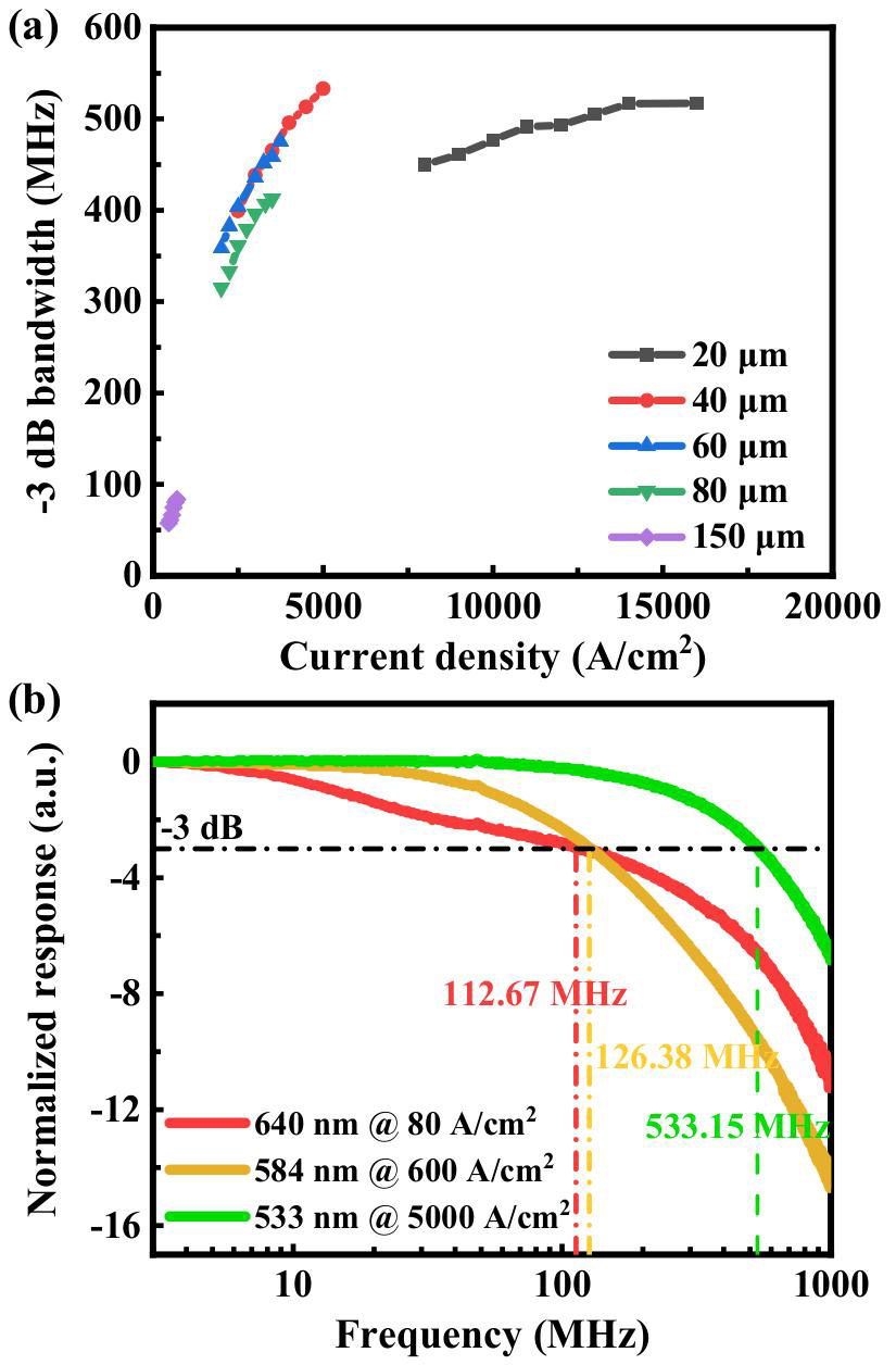
Figure 3: (a) −3dB modulation bandwidth versus current density for all five pixels. (b) Frequency responses of 40μm pixel.
The researchers comment: “Green emission exhibits higher modulation bandwidth compared to red and yellow emission, which can be attributed to the reduced carrier lifetime due to the higher operating current density required.”
The researchers also tested a proof-of-concept monolithic, multi-color wavelength division multiplexing (WDM)-optical wireless communication (OWC) scheme using emissions from three micro-LEDs with red 647nm and yellow 581nm light being supplied by 80μm pixels and green 541nm from a 40μm pixel. The respective current densities were 90A/cm2, 500A/cm2 and 1750A/cm2, and corresponding bandwidths of 79MHz, 105MHz and 324MHz.
The maximum data rates for the three channels, subject to a forward error correction limit of 3.8x10⁻³, were 486Mbits/s (Mbps) for red, 758Mbps yellow, and 1103Mbps green, or 2.35Gbps combined.
The author Mike Cooke is a freelance technology journalist who has worked in the semiconductor and advanced technology sectors since 1997.


