


News: Microelectronics
28 September 2022
Novel Crystal Technology reports first inverted gallium oxide DI-MOS transistor
At the 83rd Japan Society of Applied Physics Autumn Meeting Symposium on 21 September, Novel Crystal Technology Inc of Sayama City, Saitama Prefecture, Japan reported what it claims is the first basic operation of a gallium oxide (β-Ga2O3) inverted double-implanted MOS transistor (DI-MOSFET) with a high breakdown voltage (1kV) and a sufficiently high threshold voltage (6V). The firm has been aiming to commercialize the β-Ga2O3 transistor since 2019 by participating in the ‘Research and Development of Inverted MOS Channel Type Gallium Oxide Transistor’ program of the National Security Technology Research Promotion Fund (JP004596) of the Acquisition, Technology & Logistics Agency.
The latest achievement is expected to greatly advance the development of medium-to-high-voltage (0.6-10kV) gallium oxide transistors, in turn leading to lower prices and higher performance in power electronics. Moreover, it can contribute to the efficient use of electric energy in vehicles by improving the efficiency and downsizing of power electronics equipment such as power converters for solar power generation, general-purpose inverters for industrial use, and power supplies.
Compared with silicon carbide (SiC) and gallium nitride (GaN) as high-performance materials for replacing silicon, gallium oxide has superior material properties, and low-loss, low-cost power devices can be made with it by using a low-cost crystal growth method. β-Ga2O3 is expected to be useful in various power electronics equipment, such as home appliances, electric vehicles, railway vehicles, industrial equipment, solar power generators, and wind power generators. In addition, domestic and foreign companies and research institutes are accelerating their R&D on β-Ga2O3 because they see the material as a way to reduce the size and improve the efficiency of installed electrical equipment.
Results
Until now, normally-off β-Ga2O3 transistors have used a fin structure that does not require a p-type layer, because p-type conductive layer technology has not yet been established. However, the fin must have a fine structure of 0.4μm or less with good dimensional control. It has been difficult to fabricate devices such as this with a chip size of several millimeters square with good yield.
In response to this problem, Novel Crystal Technology has been developing an inverted MOS channel structure that can be manufactured with high yield even using conventional stepper exposure equipment and dry etching equipment. Instead of relying on developing the technically challenging β-Ga2O3 p-type conductive layer, the current development uses a high-resistance β-Ga2O3 layer doped (through ion implantation) with nitrogen (N) as an acceptor impurity, and a well layer is made through an activation heat treatment.
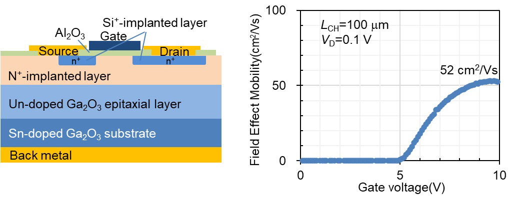
Figure 1: Cross section (left) and channel mobility (right) of long-channel lateral transistor.
In a mobility evaluation, the fabricated long-channel (LCH=100μm) lateral transistor exhibited a high threshold voltage of 6.2V (which could not be achieved with a fin structure) and a higher MOS channel mobility (52cm2/Vs) than that of a device made from silicon carbide (Figure 1).
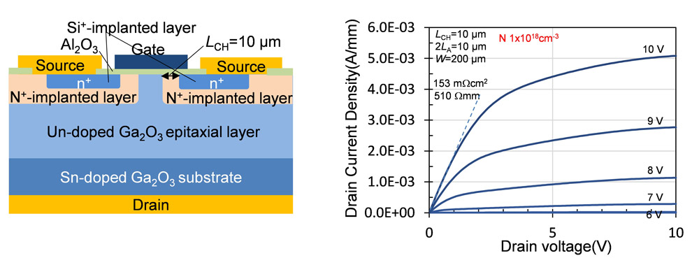
Figure 2: Cross section (left) and static characteristics (right) of β-Ga2O3 DI-MOS transistor.
Furthermore, an inverted DI-MOS transistor (Figure 2) fabricated using this process had a threshold voltage of 6.6V at an N+ ion implantation concentration of 1x1018cm-3 and an off-stage voltage of 1.1kV at an N+ ion implantation concentration of 3x1018cm-3 or higher (Figure 3). Novel Crystal Technology found that the N+ ion-implanted high-resistance β-Ga2O3 layer works as a threshold voltage control layer and a current-blocking layer in the same way as a p-type conductive layer. The researchers believe that the channel length of the prototype DI-MOSFET was as long as 10μm, and the on-resistance was as high as 153mΩcm2. The newly developed DI-MOSFET device and process should enable large devices to be fabricated on 4-6 inch wafer mass-production lines, and significant progress is expected in the development of low-loss β-Ga2O3 power transistors.
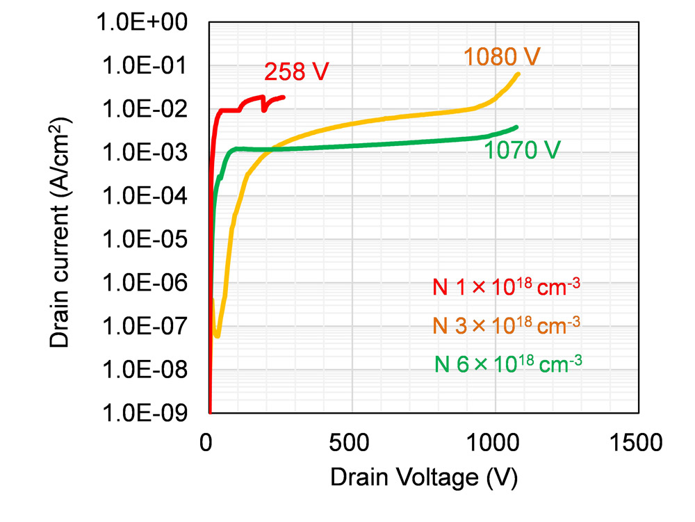
Figure 3: Breakdown voltage waveform of β-Ga2O3 DI-MOS transistor.
Future plans
Novel Crystal Technology says that it will analyze the characteristics of the N-doped β-Ga2O3 high-resistance layer in the prototype inverted MOS transistor as part of the project commissioned by the Acquisition, Technology & Logistics Agency. In addition, it aims to conduct trial production on a 4-inch mass-production foundry line, improve the device characteristics, and ensure reliability. It will also proceed with the development of a full β-Ga2O3 power module combined with a gallium oxide Schottky barrier diode (SBD) that is now being commercialized.
According to a Fuji Keizai report ‘2022 Current Status and Future Prospects of the Next Generation Power Devices & Power Electronics Related Equipment Market’, the market for medium- and high-voltage high-speed transistors and high-speed diodes is expected to grow to 7.9bn yen in 2025 and 47bn yen by 2030. Novel Crystal Technology says that it will enter this market with β-Ga2O3 transistors, SBDs, and full β-Ga2O3 modules.


