


News: Microelectronics
29 September 2022
InGaAs biristor for high-density DRAM
Researchers in Korea have demonstrated capacitor-less 4F2 2-terminal indium gallium arsenide (InGaAs) npn junction dynamic random access memory (DRAM) [Joon Pyo Kim et al, IEEE Electron Device Letters, published online 5 September 2022] with a view to highly compact 3D structures.
Standard DRAM cells tend to have areas 6-8F2 relative to the process feature size (F) that incorporate 1 transistor and 1 capacitor (1T1C). By removing the need for capacitor storage of the memory state, the cell area can be reduced. The device designed and fabricated by Korea Advanced Institute of Science and Technology (KAIST) and Korea Advanced Nano Fab Center (KANC) used a bistable resistor (biristor) structure (1R0C).
Although 4F2 capacitor-less transistor memory structures (1T0C) have been reported, they suffer from reliability problems due to hot carriers degrading the gate dielectric during operation. Birisitors produced in silicon need relatively high voltages of more than 4V to operate.
The higher mobility of III-V materials such as InGaAs enables lower voltages for a given current, and hence reduced biristor operating voltages.
The KAIST/KANC InGaAs epitaxial structure (Figure 1) was grown on indium phosphide (InP) substrate using metal-organic vapor phase epitaxy. It is hoped that present advances in integrating InGaAs on 300mm silicon substrates will lead to high-volume, low-cost deployment in future.
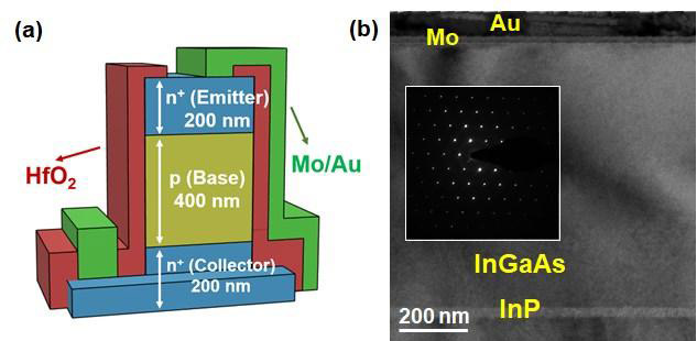
Figure 1: (a) 3D schematic structure and (b) cross-sectional transmission electron microscope (TEM) image of fabricated vertical InGaAs biristor. Inset: electron diffraction image of InGaAs material.
The n+ layer was achieved using tellurium (Te) doping with diethyl-tellurium precursor. Tellurium gives far higher activation levels of electron charge carrier concentration (ND), at more than 5x10¹⁹/cm3, compared with conventional silicon doping for n-InGaAs.
The high ND was needed for low operation voltage for the InGaAs biristor DRAM, according to design simulations. The researchers optimized the growth process to allow the use of Te doping, since compressive strains make it difficult to grow high-quality layers. X-ray analysis showed negligible lattice mismatch with the InP substrate.
The 400nm base region of the device was p-doped with zinc. The thickness of this layer controlled the operation voltage of the memory. For stable latch operation, this thickness would need to be carefully constrained in production across a memory chip, especially in the thinner layers that would result in lower operation voltage.
The fabricated devices were formed from mesas measuring 10μmx10μm. The cell area was, of course, larger. The hafnium dioxide (HfO2) surface passivation was 20nm thick. The contact metals were 20nm/70nm molybdenum/gold (Mo/Au).
The current-voltage behavior of the devices showed hysteresis with two current levels between latch-up (VLU) and latch-down (VLD) voltages. These current levels are used to represent the memory state. The latch-up state is caused by impact ionization at the base-collector junction, enabling higher current flow. As the voltage is reduced through latch-down the impact ionization stops, reducing current flow. The hysteresis behavior was only weakly dependent on temperature up to 100°C.
The team comments: “Once the biristor is latched up, the programmed state is not disturbed because of positive feedback with adequate VRead. As the device is biased with the VRead during the retention, quite large static power seems to be consumed during retention. However, it can be further reduced by decreasing the current level through device scaling.”
The researchers used program/erase (P/E) voltages of ±2.3V with write times as low as 20ns. The P/E voltage was low enough to avoid device breakdown.
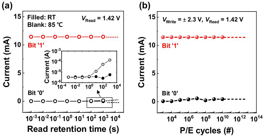
Figure 2: (a) Retention characteristics of InGaAs biristor at room temperature and 85°C. (b) Endurance characteristics.
The data retention reached more than 1000s for measurements at room temperature and 85°C (Figure 2). The endurance of the device reached to at least 1010 P/E cycles, the point at which the test was stopped. The endurance performance was attributed to the low operation voltage along with the gateless structure.
Table 1: Benchmarks with various devices reported as capacitor-less DRAM. First column: KAIST/KANC device; second column: 1T1C DRAM comparison/reference, others capacitor-less.
Characteristic |
1R0C InGaAs biristor |
1T1C Si DRAM |
1R0C Si biristor |
1T0C InGaAs transistor |
1R0C n-i-p-i-n Si biristor |
Cell area |
4F2 |
6-8F2 |
4F2 |
4F2 |
4F2 |
VWrite (V) |
2.3 |
~3.0 |
6.5 |
1 |
< 1 |
Write time |
20ns |
~10ns |
5ns |
> 30μs |
< 30 ns |
VRead (V) |
1.42 |
– |
5 |
1 |
< 1 |
Current sensing margin |
> 11.4mA (114μA/μm2) |
– |
0.42mA |
< 20μA/μm |
- |
Retention |
≥ 103s |
~64ms |
10s |
< 102s |
> 1μs |
Endurance (cycles) |
≥ 1010 |
≥ 1010 |
1011 |
< 1010 |
> 107 |
BEOL compatibility |
O (250°C) |
X |
X |
O (-) |
X |
Added to the advantages of high device reliability and scalability, the KAIST/KANC team points to the low back-end-of-line (BEOL) fabrication process temperature of 250°C as enabling of 3D device stacking for even greater concentration of memory in a small volume.
The author Mike Cooke is a freelance technology journalist who has worked in the semiconductor and advanced technology sectors since 1997.


