


News: LEDs
6 October 2022
GeSn resonant-cavity LEDs
Researchers in Taiwan report room-temperature mid-infrared resonant electroluminescence from germanium tin (GeSn) resonant-cavity light-emitting diodes (RCLEDs) with a lateral p-i-n configuration on a silicon-on-insulator (SOI) substrate [Chen-Yang Chang et al, Photonics Research, v10, p2278, 2022].
The team from National Chung Cheng University and National Taiwan University see the group IV elements GeSn as being more compatible with silicon-based electronic–photonic integrated circuits (EPICs) than hybrid or monolithic combinations with III-V light-emitting devices.
Group IV light emission is hampered by the indirectness of the bandgap, which inhibits electron-hole recombination into photons. However, the Ge energy band structure has a direct valley at the Γ point that is only 136.5meV higher than the indirect L-valley.
The team theoretically calculated that the band structure of GeSn with 4.3% Sn content and 0.52% compressive strain showed a decrease in the energy difference between the conduction-band valleys at the direct Γ point and in the L-direction to 89meV (Figure 1). The researchers comment: “Thus, the electron density populating the direct conduction band can be significantly enhanced under current injection, thereby enhancing the direct-gap light emission efficiency.”
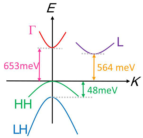
Figure 1: Calculated band structure of GeSn active layer at 300K.
The heavy-hole (HH) band peak is also raised some 48meV above the light-hole (LH) band. It has been found that GeSn with Sn content greater than 6% has a direct bandgap, but devices, including optically pumped lasers, constructed from such material tend to only perform at cryogenic temperatures so far. Achieving high Sn content is difficult due to the low solubility of Sn in Ge.
The researchers comment: “Most of the demonstrated group IV GeSn LEDs and lasers are vertical p-i-n diode structures, which suffer from a strong optical loss induced by the metal pads and heavily doped regions that could significantly increase the threshold and/or decrease the lasing temperature. To overcome this problem, lateral p-i-n structures have been proposed by keeping the lossy metal pads and heavily doped regions far away from the active region.”
Also, EPICs would be easier to achieve with lateral laser structures. EPICs have a wide range of deployments in telecommunications, on-chip optical interconnection, sensing, and quantum computing.
The RCLED material was grown by molecular beam epitaxy (MBE) on silicon-on-insulator (SOI) substrate with a Ge virtual substrate (VS) template layer (Figure 2). The buried oxide (BOX) of the substrate was 1μm, and the top silicon (Si) was 2.5μm.
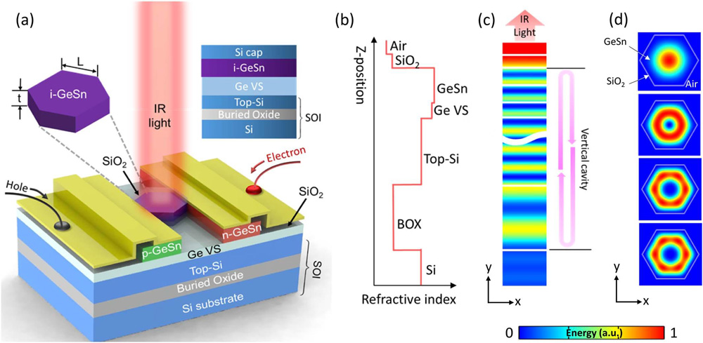
Figure 2: (a) Schematic diagram of lateral GeSn p-i-n diodes on SOI substrate. Inset: layer structure of grown sample (not to scale). (b) Refractive index profile along z direction without thin Si cap. (c) Finite element simulation of energy distribution along z direction at 1980nm, and (d) of selected transverse modes.
The VS consisted of 100nm Si grown at 600°C, 100nm Si at 350°C, 117.5nm Ge at 350°C, and 117.5m Ge at 550°C. The structure was also subject to in-situ annealing at 800°C for 5 minutes between the low- and high-temperature Ge depositions.
The 540nm GeSn with 4.3% Sn content was grown at the very low temperature (as these things go) of 150°C to avoid Sn segregation. The final Si cap was also grown at the same temperature.
Photoluminescence (PL) spectra showed a series of peaks from the resonant Fabry-Pérot cavity with an envelope maximum around 1980nm, corresponding to a photon energy of 626meV, consistent with expectations from the calculated bandstructure. The researchers assign the maximum to the lowest direct bandgap of the GeSn active layer.
The intrinsic i-GeSn layer was fabricated into a hexagonal cavity with lateral phosphorus and boron implanted p and n contact regions, respectively, forming a lateral p-i-n structure. Dopant activation was through 100s microwave thermal annealing, again avoiding Sn segregation. Plasma-enhanced chemical vapor deposition (PECVD) silicon dioxide (SiO2) was applied for surface passivation. The contact electrodes were gold/chromium.
The resonant cavity was formed from the low refractive index of the BOX and top SiO2 passivation providing vertical optical confinement. The passivation also provided horizontal confinement.
Current-voltage measurements gave a relatively high value for the series resistance of the device at 1.84kΩ. The team suggests that this is due to “the metal–semiconductor contact and the large quasi-neutral region, which may induce significant Joule heating during CW current injection.” The diode turn-on voltage was around 0.51V.
EL spectra of a device with hexagonal cavities of side (L) 20μm showed a similar series of peaks to the PL measurements (Figure 3). The envelope maximum was at the slightly shorter wavelength of 1960nm, with some red-shifting at higher currents (an effect attributed to Joule heating). The free spectral range of the emissions was around 110nm and the full-width at half maximum (FWHM) of order 70nm.
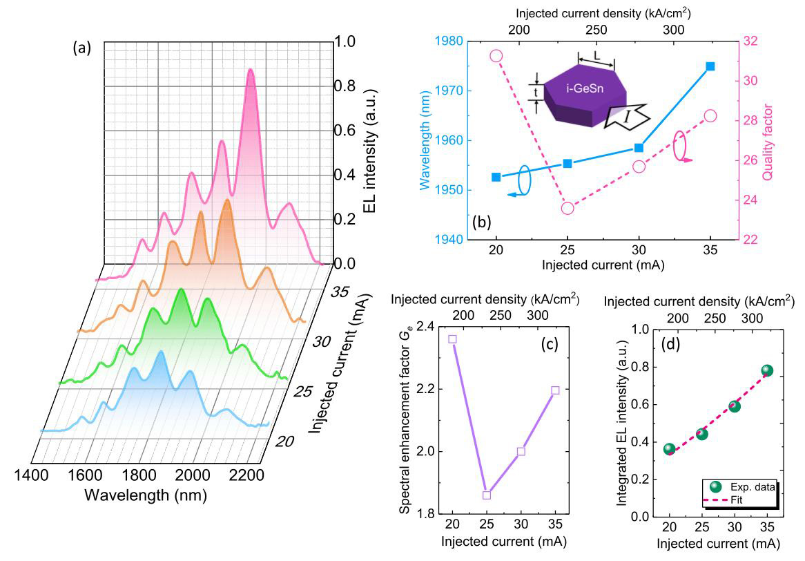
Figure 3: (a) Room-temperature electroluminescence (EL) spectra of the fabricated GeSn devices at various injected currents. (b) Extracted Q factor and resonant emission wavelength. Inset: schematic diagram of current injection into GeSn active region. (c) Spectral enhancement factor as function of injected current. (d) Integrated EL intensity as function of injected current.
Although laser emissions were not achieved, the emissions did show evidence of resonant EL, suggesting some stimulated photon transitions in addition to spontaneous photon transitions. The researchers blame the low quality (Q)-factor of the cavity for the absence of laser action. A boost to the optical confinement/Q-factor to the 100-10,000 range from Si/SiO2 distributed Bragg reflectors (DBRs) could overcome this limitation.
Increased Sn content is also another aspect that needs optimizing to further enhance the directness of the bandgap. The team suggests that the Sn content could be increased to higher than 14% by using composition-graded growth methods via MBE and CVD.
GeSn resonant-cavity LEDs GeSn SOI Substrates LEDs MBE PECVD
The author Mike Cooke is a freelance technology journalist who has worked in the semiconductor and advanced technology sectors since 1997.


