


News: Microelectronics
17 November 2022
Ethylene route to semi-insulating free-standing GaN
Researchers from China and Poland have demonstrated that halide vapor phase epitaxy (HVPE) gallium nitride (GaN) carbon-doped with ethylene (C2H4 or, showing the double bond, CH2=CH2) provides record high resistivity for creating semi-insulating free-standing substrates [Qiang Liu et al, Appl. Phys. Lett., v121, p172103, 2022].
The team from Peking University and Sino Nitride Semiconductor Co Ltd in China and Poland’s Institute of High Pressure Physics comments: “The resistivity of the sample definitely satisfies the required value (109Ω-cm) for commercially available semi-insulating GaN substrates. Therefore, such semi-insulating substrates achieved in this work will enable sharp current pinch-off for HEMT devices.”
Such substrates allow the implementation of high-performance radio frequency (RF) and microwave power amplifier applications, based on GaN high-electron-mobility transistors (HEMTs). Presently, semi-insulating silicon carbide (SiC) is often used, but the GaN/SiC lattice mismatch introduces increased dislocation densities, impacting performance. A GaN substrate would avoid the lattice mismatch problem. A peak power-added efficiency (PAE) of 82.8% has been reported for GaN HEMTs on free-standing GaN substrate.
The researchers point out that ethylene is an uncommon source for C-doping. However, their work showed that its use results in a 40x higher incorporation of C, relative to the more common methane (CH4). This may be due to the ethylene tending to decompose to CH2, breaking the double bond, before C incorporation. By contrast, methane would in the first instance dehydrogenate to CH3 radicals, slowing C incorporation into the GaN growth front.
The substrates were grown on metal-organic vapor phase epitaxy (MOVPE) 4.5μm GaN on sapphire templates (2 inch) and then separated into free-standing material by laser lift-off. The initial HVPE growth consisted of low- and high-temperature layers of GaN (960°C/1070°C) with a V/III ratio of 60. The layer thicknesses were 100μm and 50μm, respectively. The pressure was 900Torr and the source zone of the reactor was kept at 900°C.
Carbon-doped GaN layers were grown on the separated samples with the dopant sources of CH4 and C2H4 diluted by 5% nitrogen. Other factors being approximately equal, the researchers consider that the main difference in C doping from the two sources will arise from their varying chemical and physical properties.
The sample wafer ended up being 750μm thick, which was thinned down to 300μm before dicing into 10mm x 15mm test samples. The thinning was carried out from both sides, removing undoped GaN material, and double-side polishing before dicing.
The average carbon concentration in the samples, determined by secondary-ion-mass spectroscopy (SIMS), increased with dopant gas flow up to 800 standard cubic centimeters/minute (sccm): from 1.3x10¹⁷/cm3 to 1.7x10¹⁸/cm3 for methane, and 5.8x10¹⁸/cm3 to 1.5x10²⁰/cm3 for ethylene. Silicon contamination from the quartz chamber components was below 1.3x10¹⁷/cm3 at all flow rates.
In terms of input carbon atoms relative to Ga, the team estimates that the incorporation rate of ethylene was 40x higher than for methane.
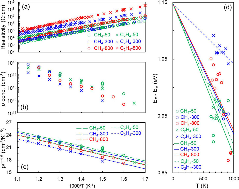
Figure 1: Temperature-dependent resistivity (a) and hole concentration (b) of all samples; (c) fitting curves for hole concentrations shown in (b); and (d) fitting curves to calculate EAV(0).
Hall-effect measurements on 5mm x 5mm testing samples showed p-type conductivity with low mobility less than 3cm2/V-s. Decreases in resistivity at high temperature arose from increased hole concentration (Figure 1). Between 315°C and 560°C, the hole concentration increased from 1012/cm3 to 1016/cm3, while the resistivity fell from 108Ω-cm to 104Ω-cm. The behavior suggests that a single impurity energy level determines the electrical properties of the sample. The team estimates the activation energy at 0K (EAV(0)) at 1.148eV. This energy corresponds to theoretical expectations for the CN0/- acceptor level. The team also found little shift in EAV above 0K, unlike for other reported research by the Institute of High Pressure Physics.
In the highest 800sccm sample doped with ethylene, the p-type conductivity was almost fully self-compensated with very low carrier mobility, making Hall-effect measurements unsuccessful.
The resistivity of GaN:C using 800sccm ethylene at 1000K was 105Ω-cm, a record compared to the previous highest for C-doped GaN of 2000Ω-cm or even iron-doped GaN at 6x10⁴Ω-cm. A problem with iron doping is diffusion to places where it is not wanted. At 833K, the GaN:C-800 had a resistivity of 6x10⁵Ω-cm, beating a report for manganese-doped GaN of 2x10⁵Ω-cm.
The author Mike Cooke is a freelance technology journalist who has worked in the semiconductor and advanced technology sectors since 1997.


