


News: LEDs
19 May 2022
AlN doping for future deep UV/power tech
Georgia Institute of Technology in the USA has reported “state-of-the-art” n-type doping of aluminium nitride (AlN) and PN AlN homojunction diodes [Habib Ahmad et al, J. Appl. Phys., v131, p175701, 2022].
The researchers comment: “This study demonstrates near-future exciting promise for AlN-based DUV [deep-ultraviolet] optical emitters and detectors, high-power/voltage/temperature, and high-frequency switching devices capable of operation in extreme radiation and heat environments.”
Up to now AlN’s extreme 6.1eV bandgap has led to its being used mainly in electrically insulating regions. A particularly attractive quality is a high thermal conductivity of 319W/mK, relative to materials such as gallium oxide (27W/mK). Also, AlN has a significantly higher critical breakdown electric field of 15MV/cm, compared with 9MV/cm for gallium oxide, 4.9MV/cm for gallium nitride, and 3.1MV/cm for silicon carbide.
The Georgia work has improved the electrical conductivity of AlN by doping with beryllium (Be) for p-AlN, based on the group’s prior work, and silicon (Si) for n-AlN.
The challenge of AlN:Si doping includes problems such as electrons being trapped at Al vacancies, threading dislocations, and ‘DX centers’. The last problem involves creating a deep state via electron capture. In the case of silicon, a secondary electron is captured, causing a geometric rearrangement with the c-axis N-bond breaking and the three other basal N-bonds shortening by 2% (Figure 1).
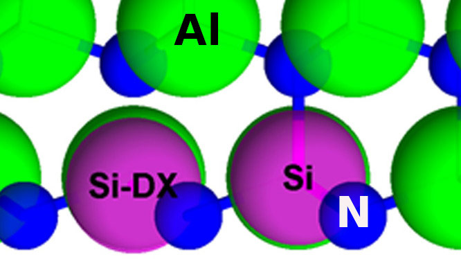
Figure 1: DX center formation of Si by transitioning to deep state compensating n-type AlN with broken N-bond in c-direction (vertical).
The researchers add: “Complicating issues, the Al-vacancy forms a complex with Si resulting in self-compensation of the doping at high Si doping levels.”
The team used metal modulated epitaxy (MME), a cyclic molecular beam epitaxy (MBE) variant, to reduce threading dislocation and Al vacancy formation. “MME compensates for the lower growth temperature with extremely metal-rich surface chemistry that virtually eliminates the harmful Al vacancies and allows easier surface bond breakage and, thus, long surface adatom diffusion lengths,” they write. A denser crystal also makes geometric rearrangements for creating DX centers less likely.
The researchers conclude: “The evidence of six orders of magnitude rectification with the proper turn-on voltage of ~6V for a 6.1eV AlN semiconductor offers ultimate confidence that the pioneering doping results shown are in fact real.”
The MME (Table 1) was performed on 4μm-thick hydride vapor phase epitaxy (HVPE) AlN on sapphire templates (MSE Supplies) using plasma-assisted molecular beam epitaxy (PAMBE) equipment (Riber 32). The templates were backed with tantalum to promote uniform heating during growth. The metalized wafers were diced into 1cmx1cm squares. Much care was taken to remove contaminants before the growth.
Table 1: Description of MME p-type AlN:Be and n-type AlN:Si films.
Doping |
Shutter cycle open/close | Growth time/cycle | Temperature | Growth rate |
| AlN:Be | 5s/10s | 6.5s | 700°C | 700nm/h |
| AlN:Si | 21s/11s | 27.3s | 800°C | 1.4μm/h |
The Al, Be and Si were sourced from standard effusion cells. The nitrogen came from an RF plasma source (Veeco UNI-bulb). The growth chamber had a high-vaccum base pressure of around 5x10-11Torr. The nitrogen beam equivalent pressure was around 1.2x10⁻⁵Torr.
The PN homojunction consisted of AlN:Be and AlN:Si, respectively. The corresponding growth rates were 700nm/h and 1.4μm/h. The researchers point out that MME has demonstrated growth rates up to 10μm/h. The III/V ratio was 1.3 in both cases.
The diode material consisted of 1μm n-AlN:Si with 8x10¹⁸/cm3 Si concentration, 200nm intrinsic AlN with 5x10¹⁷/cm3 Si concentration, and 200nm p-AlN:Be with 7x10¹⁸/cm3 Be concentration. This material was fabricated into 100μm-diameter quasi-vertical devices with annealed platinum/palladium/gold contacts.
In preliminary experiments on AlN:Si doping, the team grew material with Hall electron concentrations measured at up to 6x10¹⁸/cm3 with 7x10¹⁹/cm3 Si concentration. The team comments that this is around “6000 times higher than the previously reported state-of-the-art”.
A preliminary mobility of 17cm2/V-s is given for the 6x10¹⁸/cm3 electron concentration material, subject to “additional verification”, needed due to the contact resistance not meeting standard assumptions. Higher preliminary mobility is reported for lower electron concentrations: 370cm2/V-s at 5x10¹⁷/cm3 electron concentration (8x10¹⁸/cm3 Si).
The current through the PN diode was lower than what would be expected from contact experiments on separate AlN:Si and AlN:Be films (Figure 2). The researchers suggest this is related to problems with inductively-coupled plasma etch of the mesa during device fabrication.
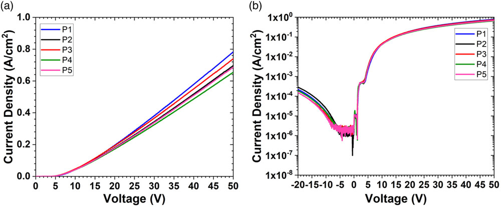
Figure 2: (a) Current density-voltage (JV) and (b) semilog JV characteristics of five equal dimension AlN homojunction PN diodes.
In particular, the team noted that the material took on a “dark tint”. The researchers comment: “This color change (presumed to be contamination) could not be removed and could introduce a combined increase in the contact resistance of the homojunction AlN diode by 3–4 orders of magnitude for two contacts.”
Both the n- and p-type layers were impacted. The current was 2-3 orders down in the n-AlN and 1 order in the p-AlN. The researchers suggest the reduced current flow in the p-AlN was due to the sub-optimal contact anneal temperature, which was focused on reducing the resistance of the n-contact. Separate annealing of the two contacts is planned to reduce the contact resistances in future work.
The forward diode performance was considered “nearly ideal except for the high series resistance owing to the aforementioned contact issues with the fabricated device.”
The turn-on voltage was around 6V, in line with expectations arising from the 6.1eV AlN bandgap. The researchers comment: “While a clear six orders of magnitude of rectification is shown, a low breakdown voltage and very high series resistance are also evident by the high current density tail on the semilog plot and the soft turn on in the linear plot.”
AlN PN AlN homojunction diodes MBE MME
https://doi.org/10.1063/5.0086314
The author Mike Cooke is a freelance technology journalist who has worked in the semiconductor and advanced technology sectors since 1997.


