


News: Suppliers
15 March 2022
Toyoda Gosei makes record diameter GaN substrates, targeting next-gen power devices
Toyoda Gosei Co Ltd of Kiyosu, Aichi Prefecture, Japan, together with Osaka University, says that it has succeeded in increasing the diameter of substrates for gallium nitride (GaN) power devices, by leveraging its expertise in GaN semiconductors such as blue LEDs and ultraviolet (UV-C) LEDs.
The firm says that higher-quality and larger-diameter GaN substrates are needed in the development of GaN power devices in order to achieve higher productivity and hence cost reductions.
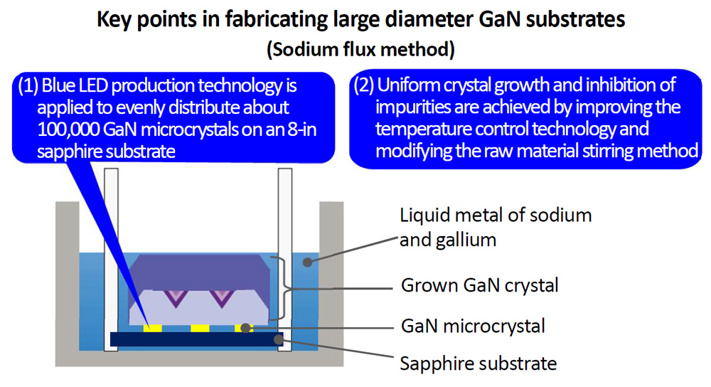
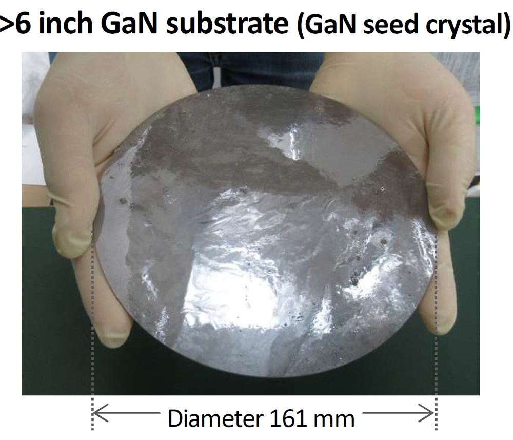
In a project headed by the Japanese Ministry of the Environment, Toyoda Gosei and Osaka University have employed a method of growing GaN crystals in a liquid metal of sodium and gallium (the sodium flux method) to fabricate a high-quality GaN substrate (GaN seed crystal) of record diameter of more than 6-inches. The researchers will next conduct quality assessments for the mass production of 6-inch substrates, and continue to improve the quality and increase the diameter (beyond 6-inches).
Toyoda Gosei’s GaN power devices chosen for Japan’s CO2 reduction project
Toyoda Gosei doubles operating current in vertical GaN power device from 50A to 100A


