


News: Optoelectronics
2 March 2022
Achieving thicker AlGaN material
Georgia Institute of Technology and Arizona State University in the USA have used non-planar growth (NPG) of aluminium gallium nitride (AlGaN) on patterned GaN on sapphire to create material with thicknesses beyond critical with a view to ultraviolet laser diodes [Frank Mehnke et al, J. Appl. Phys., v131, p073103, 2022].
Lattice mismatch and thermal expansion mismatch between AlGaN and GaN often lea to cracking of the material from the build up of stress.
The reported experimental critical thicknesses of Al0.17Ga0.83N and Al0.21Ga0.79N are less than ~620nm and ~200nm, respectively. The Georgia/Arizona work achieved laser diode structures with total AlGaN thickness ~1.5μm without cracking.
The team comments: “We believe that this approach can also be extended to NPG growth on bulk GaN substrates as well as other tensile-strained semiconductor systems.”
The templates for the work consisted of 2.7μm-thick GaN on sapphire, grown by metal-organic chemical vapor deposition (MOCVD). X-ray analysis showed the threading dislocation density in the GaN to be ~2x10⁹/cm2.
The GaN layer was patterned with 2mm-long stripe mesas of various widths between 10μm and 200μm, created using photolithography and plasma etch with silicon dioxide masking. The stripes were placed at various spacings from 10μm to 200μm. The stripes were oriented along the [1-100]GaN symmetry direction. The aim was to ease the cleaving of the material for laser facets in the perpendicular {1-100}GaN symmetry plane.
The mesa etch depth varied between 500nm and 3000nm. The deepest etch depth (3000nm) cut into the sapphire substrate. The mesa sidewalls were “near vertical”. The root-mean-square (rms) roughness was estimated at ~0.6nm on a 5μmx5μm field.
The researchers studied the MOCVD growth of 5nm-period AlGaN superlattices of various pairings of Al composition: 0.06/0.16, 0.11/0.21, and 0.16/0.26. The average compositions were 0.11, 0.16, and 0.21, respectively.
The researchers found that cracks formed in two stages: first, cracks between the stripes emerged in a [11-20] direction perpendicular to the mesa stripes; later, the cracks formed networks along the <11-20> symmetry directions.
The researchers comment: “The formation of the first cracks perpendicular to the mesa stripe orientation is most likely caused by an anisotropic strain distribution along the mesa as material can relax toward the mesa edges but is limited in relaxation along the mesa stripe.”
The team found that cracking was primarily avoided by reducing the mesa stripe width.
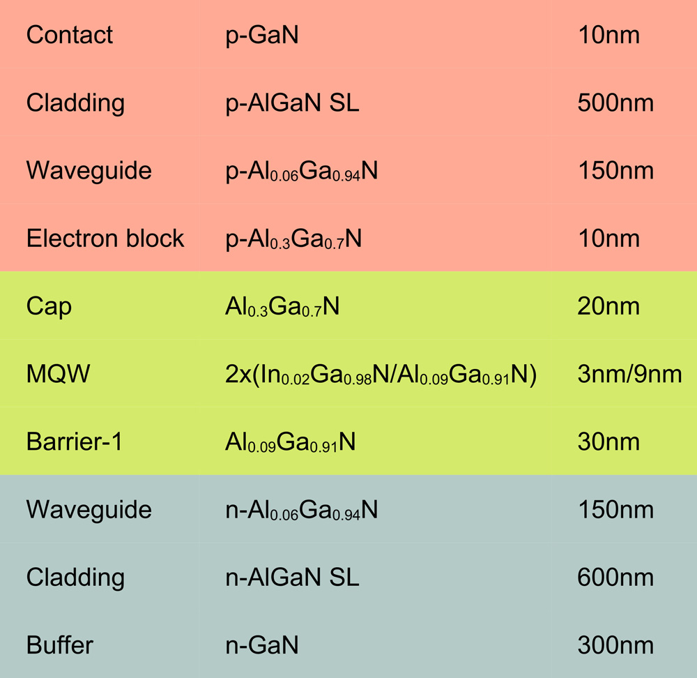
Figure 1: Structure of laser diode material.
The researchers used material grown on 2.7μm-deep mesas (i.e. 3000nm etch depth) with 100μm gap to create laser diode heterostructures (Figure 1). The superlattices (SLs) consisted of 5nm-period 0.06/0.16nm (0.11nm) Al content. The total AlGaN thickness was ~1470nm, “much larger than the critical layer thickness for these materials,” the team comments.
The researchers comment: “This heterostructure design is based upon the modeling of the optical properties of the heterostructure with the goal of increasing the optical confinement factor while not increasing the electrical resistance too much.”
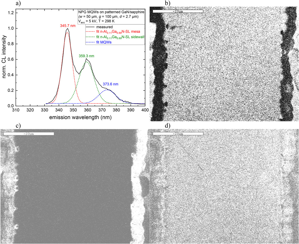
Figure 2: (a) CL spectra at room temperature of NPG MQW heterostructure and monochromatic CL maps at (b) 345.7, (c) 359.3 and (d) 373.6nm.
Under electron-beam excitation (cathodoluminescence) on material 50μm mesa widths, the structure emitted light with spectral peaks at 345.7nm, 359.3nm and 373.6nm (Figure 2). The researchers believe that these peaks were associated with emissions from the mesa, sidewall and multiple quantum well (MQW) regions, respectively.
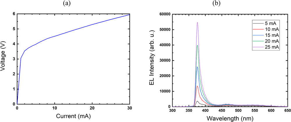
Figure 3: (a) Voltage-current plot and (b) 300K injection-current-dependent EL spectra of edge emission of a 30μm wide NPG/GaN/sapphire laser diode stripe for various DC drive currents.
Fabricated 30μmx1000μm laser diodes emitted 376.8nm electroluminescence (EL) with 13nm full-width at half-maximum (FWHM) at 25mA current injection (Figure 3). No threshold is mentioned, so one presumes that lasing was not achieved yet.
AlGaN Ultraviolet laser diodes Sapphire InGaN GaN GaN mesa MOCVD
https://doi.org/10.1063/5.0073489
The author Mike Cooke is a freelance technology journalist who has worked in the semiconductor and advanced technology sectors since 1997.


