


News: Microelectronics
22 June 2022
Gallium oxide power switching
Researchers based in the USA report record performance for metal-semiconductor field-effect transistors (MESFETs) without field plates constructed from β-polytype gallium oxide (β-Ga2O3) material [Daniel M. Dryden et al, IEEE Electron Device Letters, published online, 13 June 2022]. The record performance came in the form of an estimated Huang material figure of merit (HMFOM) of 17.5(W/C)1/2 and a 2.45kV breakdown (the latter a record for devices without field plates). The HFOM is considered “competitive with commercial wide-bandgap devices”.
The absence of field plates reduces parasitic capacitance, increasing switching speed. The team from KBR Inc., Air Force Research Laboratory, Cornell University, and Teledyne Scientific Company, see the potential for deployment in power switches and switch-mode amplifiers.
The electrical properties β-Ga2O3 have recently prompted much research as the next stage for high-voltage/high-power devices. The ultra-wide bandgap of 4.8eV results in a high critical electric field of order 8MV/cm.
The theoretical limit for the Baliga power FOM (PFOM) is 28GW/cm2, compared with 8.6GW/cm2 and 3.35GW/cm2 for gallium nitride (GaN) and silicon carbide (SiC), respectively. The HMFOM limit for β-Ga2O3 comes in at 126(W/C)1/2 (GaN: 104, SiC: 79).
The PFOM represents the trade-off between on-resistance and breakdown. By contrast, the HMFOM is aimed at the storage charge lag/resistance trade-offs involved in power-switching.
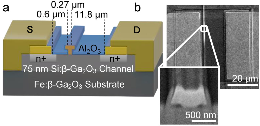
Figure 1: (a) Cross-sectional schematic of MESFET, and (b) scanning electron microscope (SEM) plan view; inset, SEM focused ion-beam cross section of scaled T-gate.
The device material (Figure 1) consisted of silicon (Si)-doped β-Ga2O3 on semi-insulating iron (Fe)-doped substrate. The device layer growth was through ozone molecular beam epitaxy. The crystal structure was (010) oriented. The substrate was supplied by Japan-based Novel Crystal Technologies. Hall measurements suggested a carrier density of 1.1x10¹⁸/cm2 and 84cm2/V-s mobility.
The device isolation was created by inductively coupled plasma etch using boron trichloride and chlorine. The ohmic contact regions were subjected to silicon implantation.
After 900°C annealing to activate the implants, the annealed source/drain (s/d) titanium/aluminium/nickel/gold electrodes were applied using electron-beam evaporation. The device was completed with a gate and s/d contact pads consisting of nickel/gold, and plasma-enhanced atomic layer deposition (ALD) aluminium oxide passivation on the channel region outside the gate. The devices were 50μm wide.
A device with 13μm source-drain distance (Lsd) had -6V off voltage, -4.2V threshold, 104 on/off ratio, and 329mV/decade subthreshold swing at 10V drain bias. The maximum drain current and peak transconductance at 10V drain bias were 60mA/mm and 26.5mS/mm, respectively. The conduction at zero gate potential was ohmic with a high resistance of 17.3mΩ-cm2 normalized to the active device area.
The breakdown (Vbk) in Fluorinert liquid came at 2.45kV, claimed as a record for β-Ga2O3 MESFETs without field plates. The average electric field between the source and drain was estimated at 2.08MV/cm. Field plates and more passivation could increase this performance, but at the cost of increasing parasitic capacitance, impacting switching speeds in applications.
The Baliga power figure of merit (PFOM, Vbk2/Ron,sp) was 347MW/cm2 (Figure 2). The researchers point out that this exceeds the theoretical performance of silicon and gallium arsenide. Further, the result is “nearly as high as record field-plated β-Ga2O3 MESFETs and a record for non-field-plated MESFETs, three times higher than the previously reported record of 115MW/cm2”.
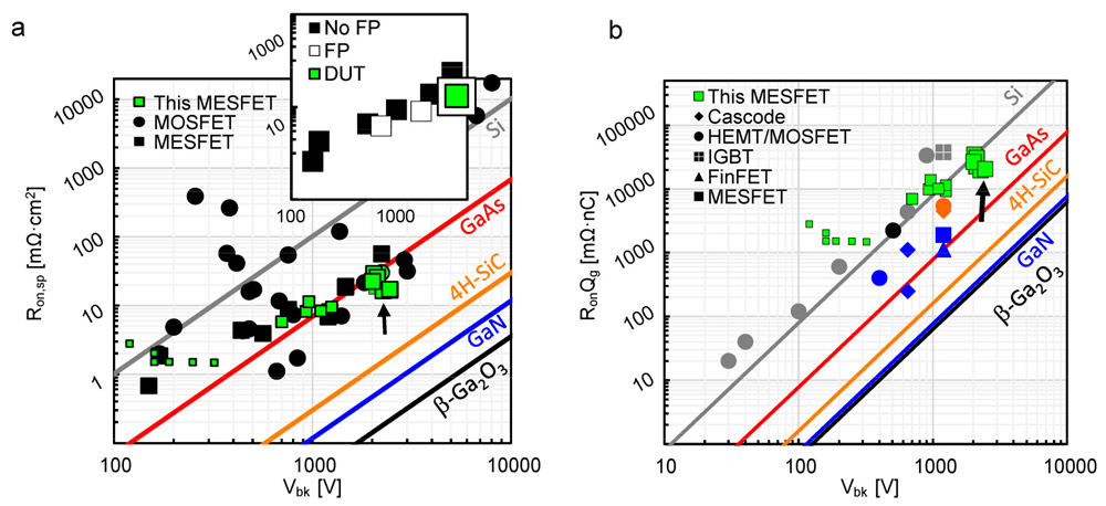
Figure 2: (a) Baliga PFOM for team’s (green) and other (black) reported β-Ga2O3 devices. Devices with Lsd of 3μm, 8μm and 13μm indicated by small, medium and large symbols, respectively. Inset: Comparison of team’s MESFET (green) to devices with (empty) and without (filled) field plates. (b) Huang’s MFOM RonQgd versus Vbk, including team’s (green) and other reported devices. Color indicates material system and shape device geometry.
The researchers seem a little puzzled by an increase of PFOM with gate-drain distance (Lgd). The team comments: “Larger devices appear to spread the applied potential over longer distances (higher depletion widths) than predicted, leading to decreased peak fields and thus higher Vbk than expected. The head of the T-gate likely provides some degree of electric field management in all devices, independent of Lgd. This observed deviation in the device depletion profile from the 1D approximation — as well as the apparent increase in average field with increasing Lgd — is not intuitive, and determining the underlying mechanism is a subject of ongoing modeling and investigation.”
There was little current collapse due to gate pulses, as seen in other β-Ga2O3 devices. The current collapse due to drain switching from 25V quiescent to 10V on was less than 30%. The researchers comment on the small gate lag: “The lack of gate oxide and its associated defect traps plays a role, though previously reported β-Ga2O3 MOSFETs also show low gate lag.”
The estimated HMFOM (μ1/2Ec=Vbk/(RonQG)1/2) was estimated at 17.5(W/C)1/2. The researchers made the estimate on the basis that the Miller charge (Qgd), 7.89pC, was the dominant contribution to the switching charge (QG). The source-side charge (Qgs) was estimated at 0.128pC. The team comments: “This estimated HMFOM is the highest reported for β-Ga2O3, competitive with commercial SiC devices, and comparable to some GaN devices but at a markedly higher Vbk.”
The researchers suggest improvements could result from lower contact resistance, self-aligned gates, and increasing carrier mobility.
https://doi.org/10.1109/LED.2022.3182575
The author Mike Cooke is a freelance technology journalist who has worked in the semiconductor and advanced technology sectors since 1997.


