


News: Suppliers
11 July 2022
LayTec presents in-situ monitoring of 2D materials epitaxy during CVD
Graphene and other sp2-bonded 2D monolayer materials like hexagonal boron nitride (hBN) and tungsten disulfide (WS2) are opening up new device and material possibilities. According to in-situ metrology system maker LayTec AG of Berlin, Germany, one of the most promising methods for synthesizing them is thermal chemical vapor deposition (CVD).
CVD process steps – precursor dissociation, adsorption, surface diffusion, island nucleation and growth – are usually thermally activated. Therefore, a reproducible process temperature measurement is of paramount importance for the control and repeatability of the deposition.
The process control frequently takes place after deposition by well-established ex-situ techniques like Raman spectroscopy, atomic force microscopy (AFM) etc. In contrast, LayTec’s in-situ metrology systems EpiTT and EpiCurve TT can be integrated into a deposition reactor and thus enable close control of key parameters during epitaxial deposition of 2D materials.
For materials that are transparent at a wavelength of 950nm like sapphire, LayTec’s EpiTT measures the temperature on the top side of the carrier. Reflectance is measured at 950nm, 633nm and 405nm. If the optical contrast between the substrate and the epilayer is sufficiently high, reflectance variations can also be measured during the growth of 2D materials with sub-monolayer coverage. In this case, the reflectance measures the surface coverage within the measurement spot, and its variation describes the different growth stages.
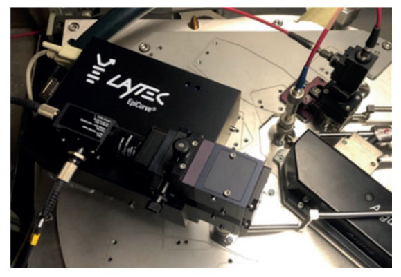
Figure 1: LayTec's EpiCurve TT mounted on an Aixtron CCS UVC reactor customized for 2D material depositions (courtesy of Aixtron Ltd.).
At the 12th Graphene and 2D Materials Conference in Aachen, Germany (5-8 July), LayTec’s Marcello Binetti presented the latest results on characterization of 2D material growth, in particular in-situ reflectance, temperature and wafer bow of graphene on sapphire during deposition. LayTec highlights some of the results achieved by monitoring graphene CVD on a single-side-polished (SSP) sapphire in Aixtron’s CCS reactor (Figure 1), demonstrating how LayTec’s metrology systems can help to increase reproducibility and yield in CVD production of 2D materials.
Figure 2 shows two runs of graphene growth on sapphire. In the first run (‘no Graphene’) the substrate only underwent the thermal cycle with temperature steps at 1347°C and 1370°C, but no precursor was injected into the chamber. In the run ‘1ML Graphene’ the sapphire substrate was heated up to 1347°C and then to 1420°C, when the deposition of 1ML graphene took place while admitting the precursor for 380s into the chamber. Then the precursor flow was stopped, and the reactor was cooled down. The 405nm reflectance tends toward a maximum, suggesting the existence of an energetic barrier for the nucleation of further monolayers.
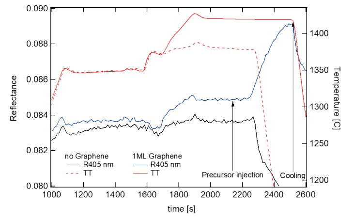
Figure 2: Data collected during two similar runs: ‘no Graphene’ and 1ML Graphene.
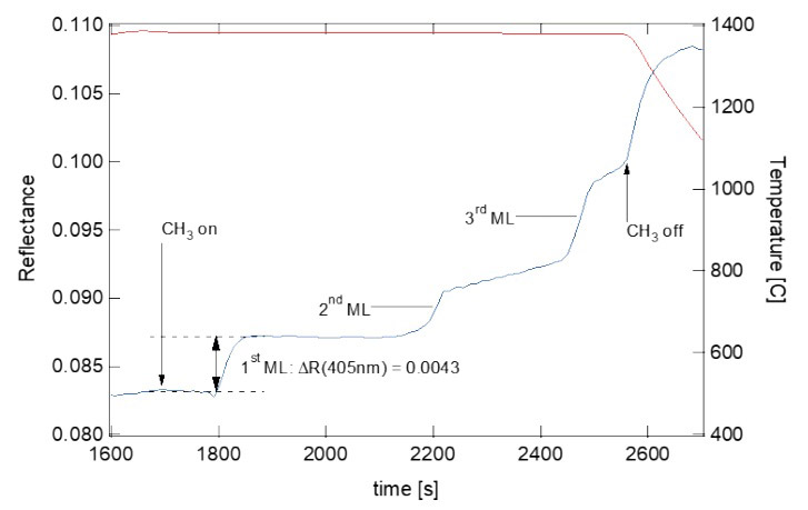
Figure 3: Evolution of ΔR405 with graphene coverage Θ between Θ=0 and Θ=3.
Figure 3 illustrates the deposition of up to 3ML graphene. After the saturation of the first monolayer, between 1900s and 2100s, the reflectance remains constant despite the availability of the precursor because an energetic barrier prevents the nucleation of further monolayers. Then, the precursor partial pressure was increased, allowing the controlled growth of the second and third monolayers. This process is mirrored by the increase in R405.
To verify the results, ex-situ Raman spectroscopy measurements were performed which confirmed the presence of 1-2ML of graphene and 3ML of graphene on the two samples. Consequently, wafer temperature and surface coverage can be directly deduced right during deposition, which ensures accurate process control. Moreover, measuring the variation of the surface reflectance during the growth reveals details on the deposition kinetics and enables tighter control of the number of deposited monolayers already during the process.
LayTec concludes that its EpiTT and EpiCurve TT allow in-situ monitoring of 2D materials deposition and offer new means for controlling these complex processes, accelerating research on 2D materials and scale up for industrial production.


