


News: Microelectronics
21 July 2022
Buffers for GaN power on AlN substrate
Researchers based in Belgium and Germany report on gallium nitride (GaN) buffer structures on 200mm polycrystalline aluminium nitride (poly-AlN) substrates aimed at >1200V hard breakdown power applications such as electrical vehicles [Anurag Vohra et al, Appl. Phys. Lett., v120, p261902, 2022].
One advantage of using poly-AlN as a substrate is that the coefficient of thermal expansion is much closer to that of the GaN/AlGaN used in buffers than for other substrates, such as silicon Si (111).
According to the team from Belgium’s Imec vzw, Germany’s Aixtron SE, and CMST imec and Ghent University in Belgium, this paves the way to thicker buffer structures on large-diameter substrates, while maintaining and enabling higher-voltage operation.
The researchers used Imec’s proprietary reversed stepped superlattice (RSSL) buffer scheme. They comment: “The RSSL buffer scheme features a much larger flexibility in stress engineering and, hence, becomes a more promising candidate for the growth of thick buffer structures on the engineered substrates of large size, which show different mechanical behaviors than regular silicon substrates.”
The researchers used 200mm engineered poly-AlN “Qromis Substrate Technology” (QST) substrates supplied by Qromis Inc. The epitaxial growth was performed in an Aixtron G5+ C planetary reactor. The growth substrates included a Si (111) top layer bonded to the QST poly-AlN by silicon (di)oxide (SiO).
The RSSL buffer stacks (Figure 1) were grown with (Ex C-doped) and without intentional carbon doping. Of course, in metal-organic chemical vapor deposition (MOCVD) some intrinsic C-doping is almost unavoidable. One can affect this intrinsic C incorporation by tuning of the growth temperature V/III (N/AlGa) ratio, for example.
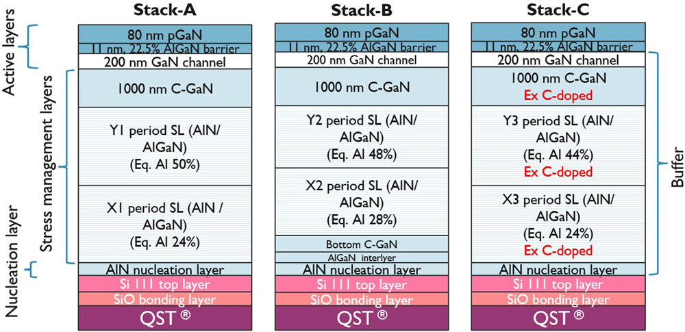
Figure 1: High-electron-mobility transistor (HEMT) stacks based on intrinsic (stack A and stack B) and extrinsic (stack C) C-doping. Buffer thicknesses of stack A and stack B varied from 5.3-7.4μm to 4.8-6.1μm, respectively. Stack C had a thickness of ~6.8μm.
The aim of the work was to maximize the breakdown voltage of the buffer stack through optimizing the Al contents, C-doping and buffer thickness. Higher Al content should increase the critical field for breakdown. Thicker buffers should have a lower field at the AlN/Si nucleation interface for a given potential. The layers were designed to manage the stress and thus avoid excessive wafer bowing.
The researchers were unusually relaxed about a high threading dislocation density emanating from the AlN/Si nucleation interface: “Defect control has not been focus of this study as it is known on the contrary that large density of these defects might actually help to reduce the dispersion for intentionally C-doped buffers.”
Low dispersion is a key need of dynamic power management where the device performance needs to be almost the same as in DC operation when switched on and off, and for recovery from high voltage stress.
The vertical breakdown of the buffers was measured at 25°C and 150°C. The target limits for leakage current density were 1μA/mm2 and 10μA/mm2, respectively.
Stack A with 7.2μm thickness met the target of more than 1200V , but there was asymmetry in the breakdown voltage for forward bias and reverse bias, a difference of 300V at 150°C.
Stack B only managed a ~900V breakdown rating for 6.1μm thickness, but the team is confident that a thicker 7μm stack with this structure could meet the 1200V requirement. On the plus side, the performance was more symmetrical between forward and reverse biasing. The researchers attribute this to the insertion of bottom C-GaN and AlGaN interlayers.
The extrinsic C-doped stack C showed negligible difference in current-voltage performance in forward and reverse bias. The researchers attribute this to the tuned and uniform C concentration across the wafer.
For stacks A and B the non-uniformity in C concentration caused the center part of the wafers to have lower breakdowns than the mid and edge regions. The team expects that improvements in uniformity could be seen from adjusting local V/III ratio and flow distributions.
The researchers prefer the extrinsic doping approach, commenting: “Adjusting the C-level by an intrinsic doping level requires unfavored process conditions for crystal quality and limits the process parameter space significantly. As a preferred choice, the C-level and uniformity can be controlled by using an external C-doping source. This allows a very wide process window and combines very high crystal quality with C-density optimized for high breakdown and with little to no buffer dispersion.”
Stack C met the 1200V rating at 25°C, but exhibited some failures in the 1000-1100V range at 150°C. The researchers comment: “The root cause for these sudden failures is not yet understood. For the moment, we can exclude extrinsic C-doping as the origin of these failure, as earlier experiments in GaN-on-Si have shown improved device yield.”
The team believes that the higher temperature would also meet the 1200V rating for all test structures at 150°C if the thickness were increased from 6.8μm to 7.2μm.
Two-dimensional electron gas (2DEG) transmission line method (TLM) structures (Figure 2) were used to find the dispersion of the buffers. Resistances before and after a 10s back-gate negative bias were compared to give the dispersion.
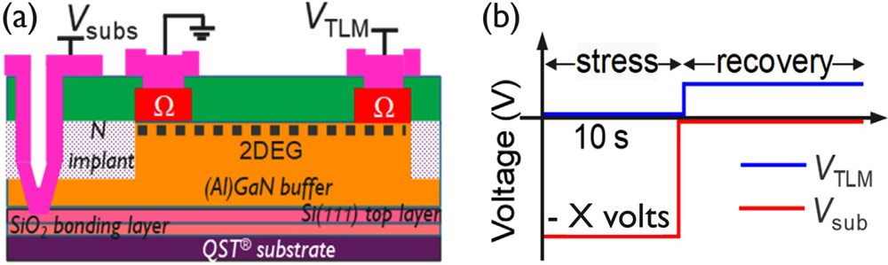
Figure 2: (a) Test structure and (b) test procedure to measure buffer dispersion. X varies from -650V to -1200V, depending on stack thickness.
For stack A the dispersion was in the range ±25%. For stack B the range was ±5%, but the back gate stress was -900V rather than -1200V. The team comments: “The extrinsically C-doped stack C shows advantages over the intrinsic doping in stack A with a very narrow distribution for buffer dispersion even at -1200V.”
The dispersion range was below 7% for stack C, both at 25 and 150°C.
GaN buffer structures Poly-AlN substrates MOCVD
https://doi.org/10.1063/5.0097797
The author Mike Cooke is a freelance technology journalist who has worked in the semiconductor and advanced technology sectors since 1997.


