


News: Microelectronics
20 January 2022
Boosting transconductance and squeezing off-current
National Yang Ming Chiao Tung University in Taiwan has reported increased transconductance (gm) and reduced OFF-current (IOFF) for indium gallium arsenide (InGaAs) fin field-effect transistors (FinFETs) from remote nitrogen plasma passivation of the gate insulation layers [Hua-Lun Ko et al, IEEE Transactions on Electron Devices, published online 20 December 2021].
The devices were fabricated from n+-InGaAs on heavily p-type indium phosphide (p+-InP). The source/drain regions were doped with silicon implantation and activation annealing. The fins were etched with plasma, followed by citric acid sidewall smoothing and fin-width shrinking. The fins were oriented in the (010) crystal direction to give the highest aspect ratio.
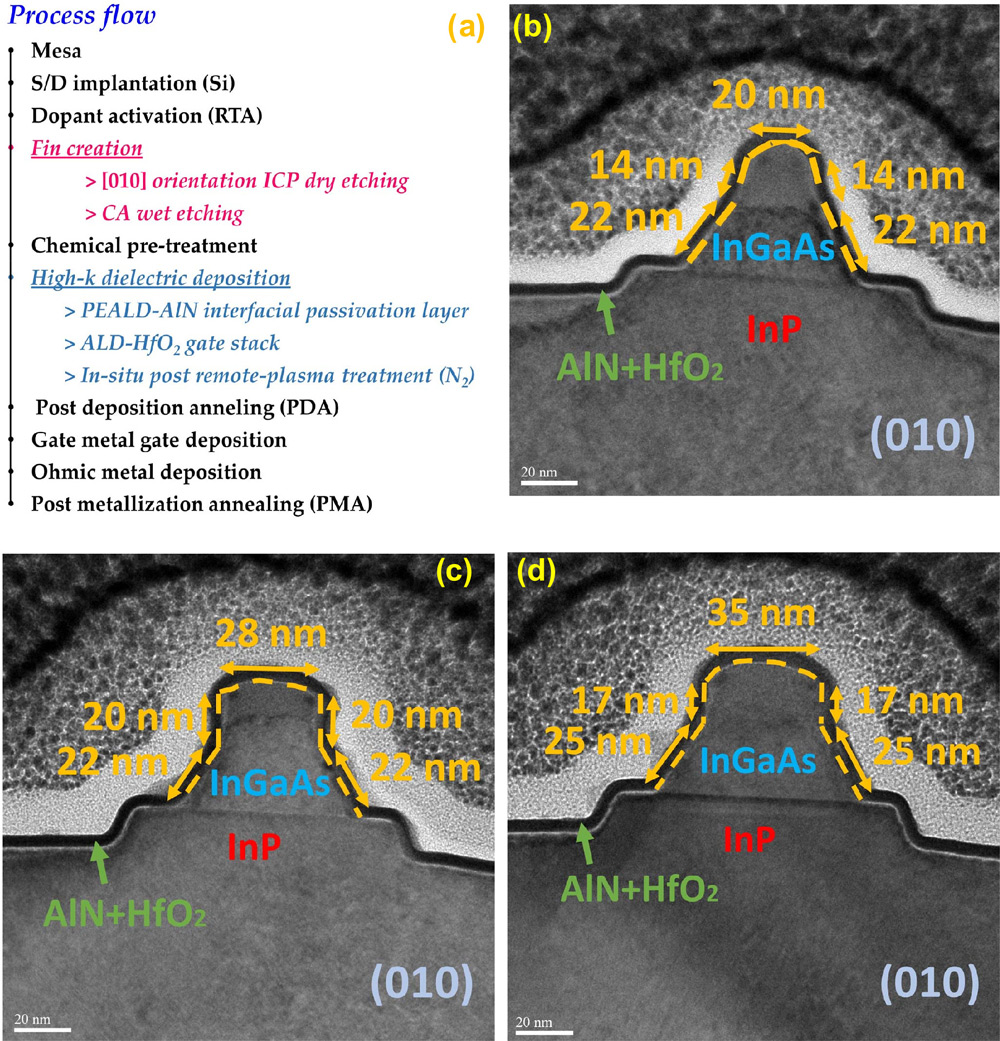
Figure 1: (a) FinFET fabrication. Cross-sectional high-resolution transmission electron microscope images of fins of width 20nm, (c) 28nm and (d) 35nm.
The gate insulators consisted of 0.8nm aluminium nitride and 2.9nm hafnium dioxide, both applied using atomic layer deposition (5 cycles and 30 cycles, respectively). The insulation was treated with nitrogen (N2) remote plasma (RP) in-situ to fill oxygen vacancies in the high-k materials. This reduced the OFF-current density in all devices to less than 5x10⁻⁴μA/μm. Further, the team comments: “Additionally, trap-assisted tunneling (TAT) and Frenkel–Poole emission are greatly inhibited by N2 RP passivation.”
The researchers estimate that the equivalent oxide thickness of these high-k layers is 0.8nm.
The devices were completed by annealing at 450°C in forming gas (hydrogen/nitrogen mix), gate metal deposition, ohmic source/drain metalization, and post-metalization annealing.
The resulting devices demonstrated high ON-current and peak transconductance (Figure 2). “The devices fabricated in this work showed highest gm of 2727μS/μm, highest ION of 835μA/μm, high Q-factor (Q = gm/SSsat) of 22.3, high ION/IOFF current ratio of 3x10⁵, and low OFF-current of 4.5x10⁻⁴μA/μm for Lch = 45nm and Wfin = 35nm N2-passivated In0.53Ga0.47 As FinFETs,” the team reports.
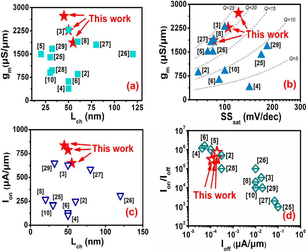
Figure 2: Benchmark plots of (a) peak gm versus channel length (Lch), (b) peak gm versus subthreshold swing (SS) in saturation regime, (c) ION at VGS–Vth = 0.5V and VDS = 0.5V versus Lch , and (d) ION/IOFF ratio versus OFF-current. Data compared with other state-of-the-art In0.53Ga0.47As FinFET devices.
At 0.5V drain bias (VDS), the subthreshold swing (SS) was as low as 78mV/dec, and drain-induced barrier lowering (DIBL) was 55mV/V. Reducing the drain bias to 0.05V allowed even lower OFF-currents of 1.13x10⁻⁴μA/μm.
InGaAs FinFETs Remote nitrogen plasma passivation
https://doi.org/10.1109/TED.2021.3133222
The author Mike Cooke is a freelance technology journalist who has worked in the semiconductor and advanced technology sectors since 1997.


