


News: Microelectronics
17 February 2022
Reliable 0.25μm GaN HEMTs for X-band applications
US-based Wolfspeed has reported improved reliability, voltage rating, and output power of 0.25μm-gate gallium nitride (GaN) high-electron-mobility transistors (HEMTs) from implementing a sunken source-connected field-plate (FP) [Kyle M. Bothe et al, IEEE Electron Device Letters, published online 24 January 2022].
The estimated mean time to failure (MTTF) of Wolfspeed’s new sunken FP design (Figure 1) was 6x10⁷ hours at 225°C junction temperature, beating the performance of previous reports, while maintaining a high output power density. The device is aimed at X-band 8.0-12.0GHz microwave applications such as high-power wide-band radar and communications.
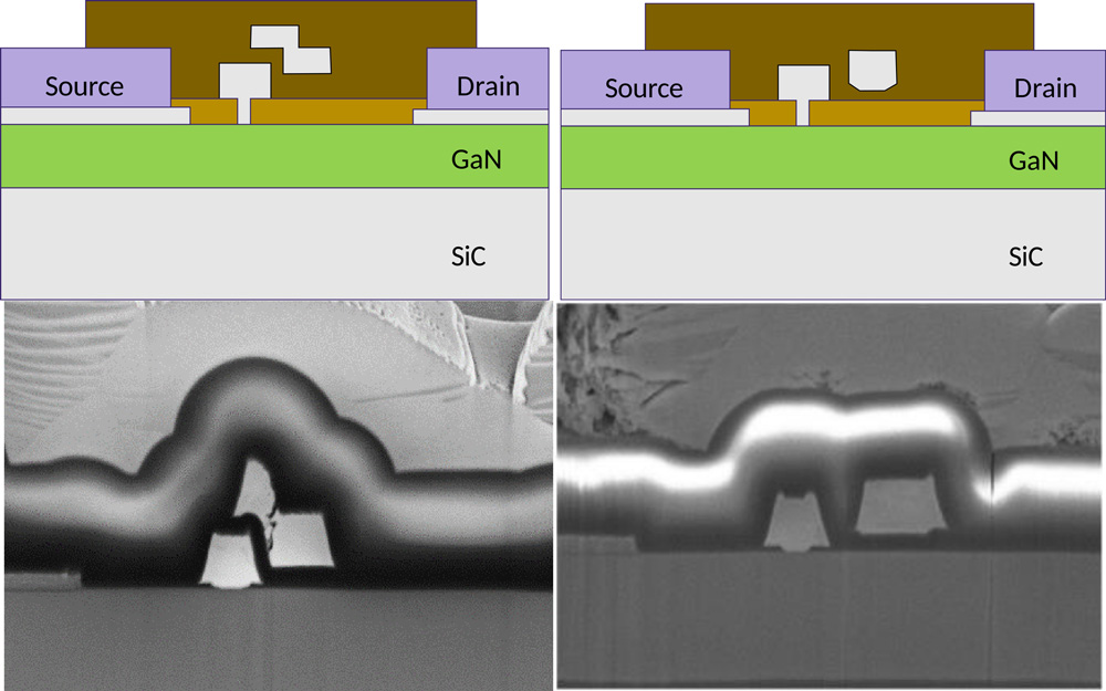
Figure 1: Schematic and fabricated cross sections of (a) standard field-plated GaN HEMT and (b) novel sunken source-connected field-plated HEMT.
Field plates are used to reduce the peak electric field for a given bias condition, enabling higher breakdown voltages to be achieved. Hence the drain bias (VD) rating can be increased, allowing higher saturated output powers (Psat) to be reached. Further benefits were increased linear gain and power-added efficiency (PAE).
The researchers comment: “Positioning the sunken field plate closer to the channel enhances the Faraday shielding effect to block the parasitic fields connection between the gate and drain. Furthermore, the trapping of the device was improved by optimizing the trench etch chemistry and resulting trench profile.”
Wolfspeed used its own 0.25μm HEMT foundry to fabricate the devices, including layers for passive devices aimed at monolithic microwave integrated circuit (MMIC) production. The metal-organic chemcal vapor deposition (MOCVD) of GaN and aluminium gallium nitride (AlGaN) on silicon carbide (SiC) was optimized for 10GHz performance with a view to reliable and robust high-volume manufacturing. The 1.4μm insulating iron-doped GaN buffer was grown on an AlN nucleation layer. The AlN barrier layer was less than 2nm. The material was capped off with 18nm AlGaN.
The researchers comment: “The thickness of the AlGaN cap was chosen to ensure that the gate-length to barrier ratio maintained the correct aspect ratio to minimize short-channel effects.” The thick AlGaN cap also blocked gate leakage current, removing the need for a conventional GaN cap layer.
The material structure resulted in a two-dimensional electron gas (2DEG) under the barrier layer with a 1.2x10¹³/cm2 electron density and 2000cm2/V-s mobility, resulting in a sheet resistance of ~270Ω/square.
The device fabrication used a gold-free alloy for the recessed source/drain electrodes. Recessing avoids the need for GaN regrowth and results in a low-profile height contact.
The gate fabrication process used silicon nitride passivation. A shrink method developed by Wolfspeed was implemented to enable the 365nm-wavelength i-line lithography to achieve the 0.25μm gate length. The gate was placed off-center in the 4.5μm gap between the source/drain electrodes.
The field plates were added after the gate, also using i-line lithography. The 0.95μm sunken field plate was offset by 0.15μm from the T-gate edge. The relatively large size of the field plate minimized the gate-drain capacitance (Cgd), fully covering the gate-drain trench, at the cost of a slight increase in drain-source capacitance (Cds). Devices with a conventional 0.8μm field plate, overlapping the gate by more than 2μm, were fabricated on the same wafer, allowing fair comparison with respect to process variations.
Table 1: Comparison of HEMT performances.
| Parameter | Units | Standard FP | Sunken FP |
| Ron | ohm-mm | 2.3 | 2.3 |
| gm | mS/mm | 370 | 370 |
| Vp | V | -2.8 | -2.8 |
| VBD | V | > 120 | > 150 |
| Cgs | pF | 1.36 | 1.15 |
| Cgd | fF | 34 | 14 |
| Cds | fF | 200 | 230 |
| Gain | dB | 17 | 19 |
| PAE | % | 57 | 64 |
| Psat | W/mm | 7.8 | 10.6 |
| VD Rating | V | 40 | 50 |
| Lifetime (225°C) | hours | < 1E6 | > 6E7 |
The devices were thinned to 100μm and connections made through backside slot vias before testing (Table 1). Improved trapping and radio frequency performance was indicated in comparisons between DC and pulsed operation with the drain current reduction of 23% for the standard FP decreasing to 18% for the sunken FP. The new sunken FP structure also resulted in better, generally lower, parasitic capacitances and higher breakdown voltage (VBD).
RF accelerated life tests at 3.5GHz were carried out on devices with 3.6mm periphery. The temperature was raised during testing to give three junction temperatures in the 360-425°C range. The quiescent drain current was 200mA. The input power was 29dBm. The lifetime was determined by catastrophic failure or a 1dB reduction in Psat. Using an Arrhenius temperature-accelerated lifetime model, the researchers estimate a more than 6x10⁷ hour lifetime at 225°C junction temperature. “This is a more than two orders of magnitude increase over the conventional field-plate design,” the team points out.
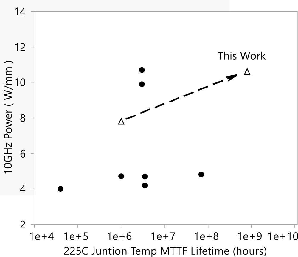
Figure 2: Comparison of leading 10GHz RF power 0.25μm GaN HEMTs with respect to MTTF device lifetime.
The sunken FP design enables Wolfspeed to both beat existing mean-time-to-failure estimates of previous reports on 0.25μm GaN HEMTs while maintaining power density (Figure 2).
GaN HEMTs GaN HEMTs X-band AlGaN SiC MOCVD
https://doi.org/10.1109/LED.2022.3146194
The author Mike Cooke is a freelance technology journalist who has worked in the semiconductor and advanced technology sectors since 1997.


