


News: Optoelectronics
23 February 2022
InGaAs/colloidal nanocrystal infrared detector
Researchers in France have combined indium gallium arsenide (InGaAs) III-V nanowires with colloidal mercury telluride (HgTe) II-VI nanocrystals (NCs) to create a photodiode sensitive to light in the 1.6-2.0μm short-wavelength infrared (SWIR) range [Adrien Khalili et al, Appl. Phys. Lett., v120, p051101, 2022].
The team from Sorbonne Université, ONERA-The French Aerospace Lab, and University Lille, comment: “For a long time, the design of IR sensors has opposed narrow-bandgap III–V semiconductors against their colloidal II–VI counterpart. Here, we demonstrate that Van der Waals heterostructures can be obtained from these two types of semiconductors.”
Typical Van der Waals heterostructures include graphene and transition-metal dichalcogenides. It is hard to see how these structures can be scaled up to mass production from laboratory-scale flakes measuring at most a few tens of microns. By contrast, large-production-scale III-V materials are basic to ubiquitous light-emitting diodes and laser diodes.
Narrow-gap nanocrystals such as HgTe are used to absorb the infrared tail of the solar spectrum in photovoltaic devices and in infrared cameras.
The InGaAs nanowires were produced using selective-area molecular-beam epitaxy on indium phosphide substrate. The mask was plasma-enhanced chemical vapor deposition (PECVD) silicon dioxide, resulting in an array of 200 nanowires of 200μm x 130nm dimensions with 500nm pitch. The wires were coupled with a few nanowires in the perpendicular direction to reduce the resistance (Figure 1). The n-type doping level of the array was 5x10¹⁸/cm3.
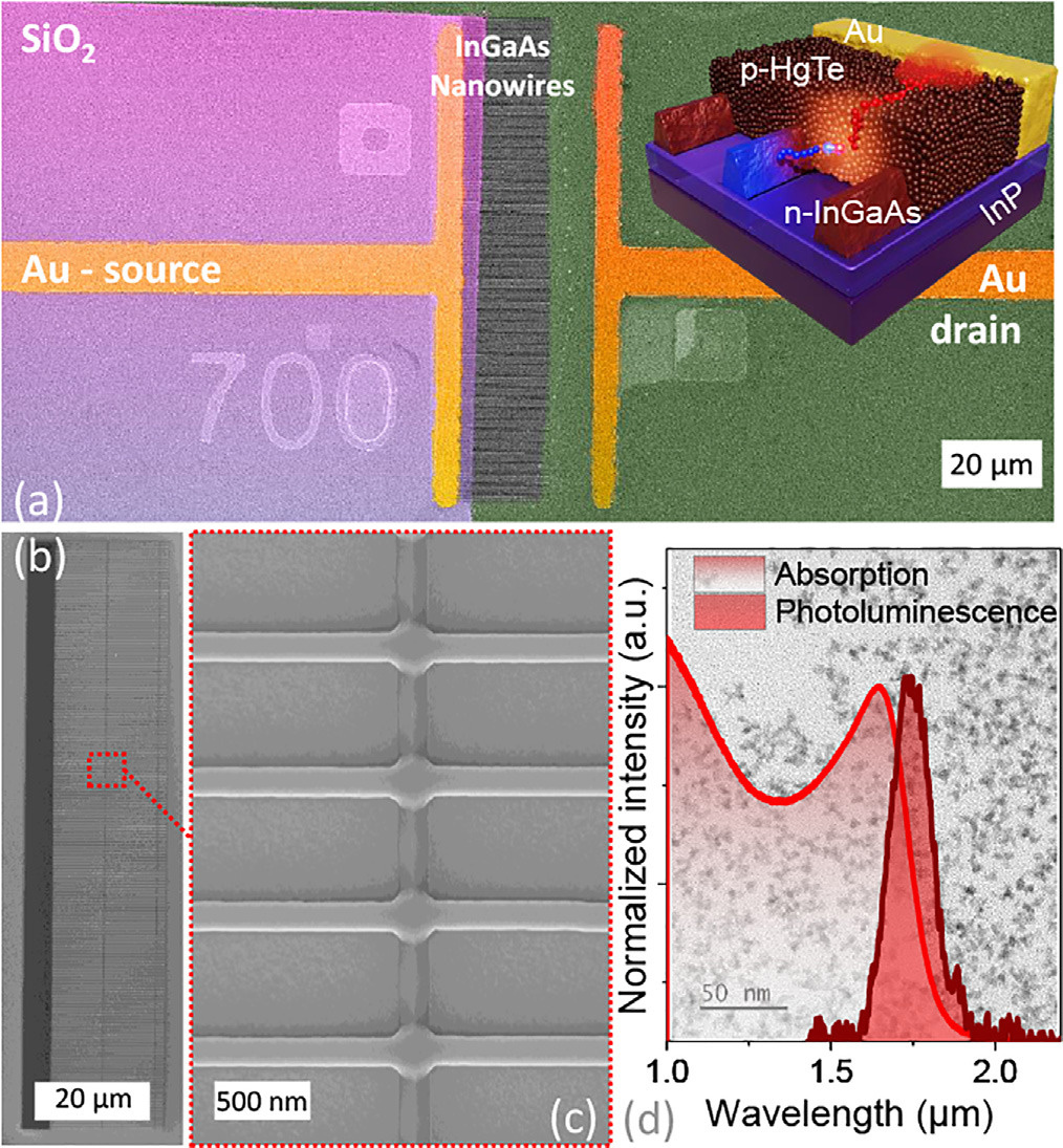
Figure 1: InGaAs wires/HgTe NCs hybrid device. (a) False color microscopy image of patterned nanowires. Right inset: schematic device with HgTe nanocrystal film. (b) Scanning electron microscope image of InGaAs wire array. (c) Zoomed InGaAs wire array image. (d) Normalized absorption and photoluminescence spectra of HgTe nanocrystals. Background: transmission electron microscope image of HgTe nanocrystals.
Gold was deposited to give source/drain metal electrodes with the source connected to the nanowires. A silica patch (purple false color in Figure 1) was placed over the connection between the source and the nanowires, separating the electrode from the HgTe NC layer. The drain was not connected to the nanowires.
The device was then coated with a 200-400nm HgTe NC layer. The target NC diameter was 8nm, which gives a 2μm wavelength band edge. This was red-shifted relative to that of the InGaAs nanowires, 1.6μm. Peak photoluminescence was around 1.7μm (≈700meV). The film becomes conductive through ligand exchange reactions, giving a 2μm cut-off.
Separate electrical measurements on the InGaAs and HgTe materials gave ohmic behavior. Hall measurements on the InGaAs resulted in 3000cm2/V-s electron mobility. Field-effect analysis of the HgTe NC material showed conduction only by thermally activated holes. The activation energy was ≈200meV.
The InGaAs nanowire/HgTe NC film combination gave a diode structure with a strongly rectifying current-voltage characteristic. The activation energy of the charge transport increased to 400meV (down to 200K), suggesting strong reduction of dark current through device cooling.
Under illumination there was no open-circuit voltage (VOC) observed. “This lack of VOC prevents device operation under 0V bias,” the team comments.
The researchers attribute the zero VOC to shunt resistance in NCs along the nanowires. “This can come from hole conduction beginning at the interface between the wire and the nanocrystals up to the contact electrode and from a possible recombination of photogenerated carriers when the latter travel along the long n-type wires,” they explain.
However, the strong rectification and low dark current allows the reverse bias to reach -4V, in contrast to other diode structures involving HgTe NCs, which are limited to reverse biases smaller than 0.4V, due to a loss of current-voltage asymmetry.
Photocurrent spectroscopy and simulation analyses suggest that the HgTe nanocrystal film accounted for the bulk of the photon absorption. The InGaAs nanowires behaved as a unipolar barrier extracting photoelectrons.
The team comments: “This simple strategy expands the spectral response of the InGaAs by 400nm (from 1.6 to 2μm cutoff wavelength).”
The infrared response was measured under a variety of biases, temperatures, illumination powers, and modulations (Figure 2). The responsivity at 300K reached 16mA/W at -4V bias. Although the response was only weakly dependent on bias sign, the dark current was minimized with reverse bias, and hence is preferred. Although cooling to 200K reduced the response by a factor of 2, the dark current was reduced by three orders of magnitude.
Charge conduction in the nanocrystal layer is thought to occur by a thermally activated hopping mechanism. The researchers add: “Under illumination, the carrier density is set by the incident photon flux, and thus the temperature dependence of the response is mostly the result of the thermal activation of the carrier mobility.”
The noise behavior seems 1/f limited, rather than white (shot and thermal). This suggests that the source is the nanocrystal layer, rather than the InGaAs nanowires. This resulted in a specific detectivity of 7x10⁷Jones at room temperature, and 109Jones at 200K (Figure 2d).
Although the detectivity does not reach the level of state-of-the-art diodes based on HgTe nanocrystals, up to 1011Jones at room temperature, the result is comparable to a reported device consisting of HgTe nanocrystals on graphene (108-109Jones).
The team comments: “Certainly, our approach suffers from the lack of VOC preventing the zero-volt operation. On the other hand, thanks to its planar geometry, that is associated with a weaker capacitance than the vertical geometry diode, fast operation can be achieved.”
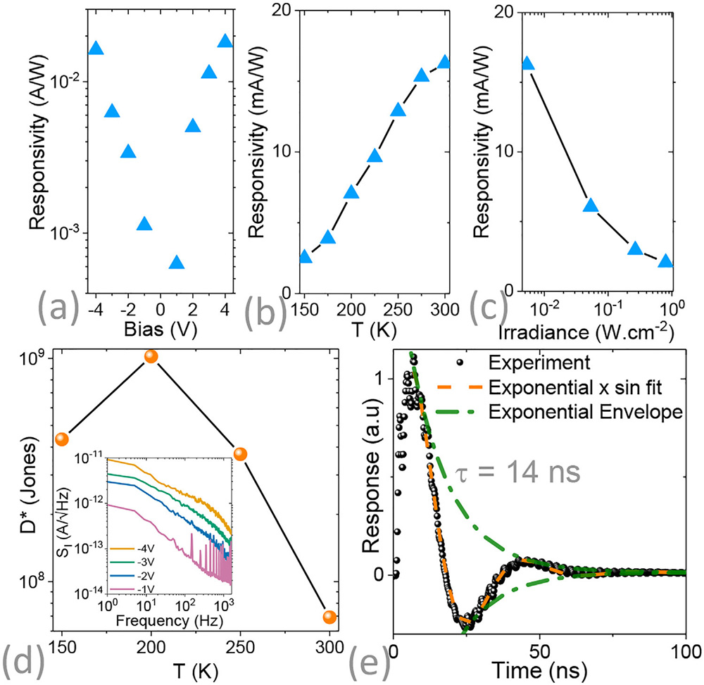
Figure 2: Photodetection performance of hybrid structure. (a) Responsivity at 300K as function of applied bias, under 1.55μm 5mW/cm2 laser-diode illumination. (b) Responsivity as function of temperature at -4V bias. (c) Responsivity as function illumination power at -4V bias. (d) Specific detectivity at -4V bias as function of operating temperature for 1kHz signal. Inset: noise current spectral density as function of signal frequency with device under various biases. (e) Photocurrent response to 1ns pulse at 1.57μm wavelength. Fit provided by ≈14ns exponentially decaying sine wave, accounting for imperfect impedance matching of device with acquisition oscilloscope.
In fact, the 14ns decay response to 1ns pulses (Figure 2e) is two orders of magnitude lower than reported values for vertical diodes. “In this sense, the weaker signal-to-noise ratio is balanced by a higher device bandwidth,” the team comments.
The researchers hope future work will “combine the architecture with gate control and light management to further enhance the signal-to-noise ratio”.
InGaAs Colloidal nanocrystal infrared detector III-V nanowires HgTe SWIR PECVD
https://doi.org/10.1063/5.0076708
The author Mike Cooke is a freelance technology journalist who has worked in the semiconductor and advanced technology sectors since 1997.


