


News: Optoelectronics
10 February 2022
Intermediate anneal therapy for QWs
China’ Institute of Semiconductors has used an intermediate annealing process between growing quantum wells (QWs) and barriers to improve the performance of indium gallium nitride (InGaN) laser diodes (LDs) and light-emitting diodes (LEDs) [Feng Liang et al, Optics Express, v30, p3416, 2022].
Although the wavelengths of the reported devices were in the III-nitride violet ~400nm-wavelength comfort zone, it is hoped with development to extend the wavelength range down to near-infrared (~700nm). Already III-nitride light-emitting devices power laser display, laser lighting, laser processing, laser medical treatment, and underwater communication applications. Improving the well/barrier interface with annealing should enhance luminous efficiency, further increasing the deployment of III-nitride technology.
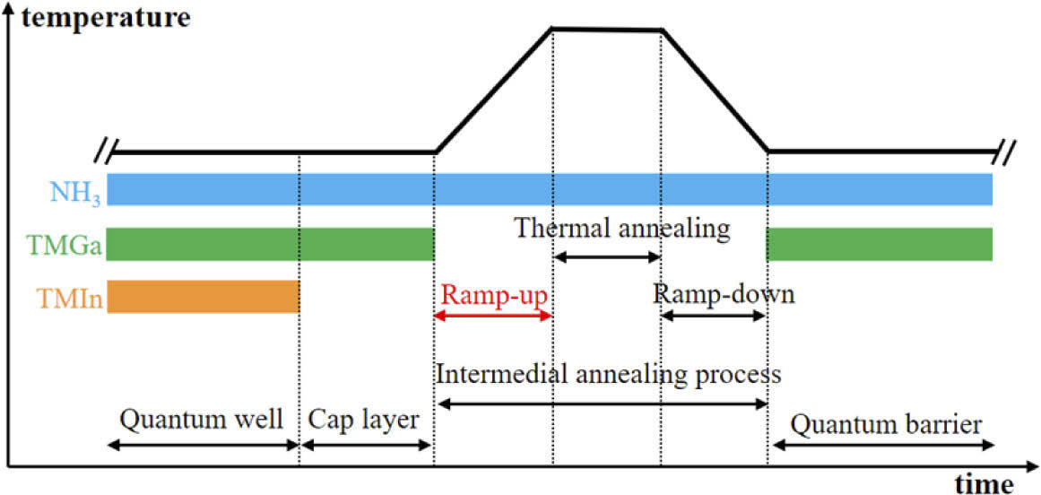
Figure 1: Time-dependent temperature process and gas flow schemes during MQW growth.
The researchers applied a thermal annealing step of several seconds between the InGaN well and GaN barrier metal-organic chemical vapor deposition (MOCVD) growth sequences (Figure 1). The MOCVD process used trimethyl-gallium (TMGa) and trimethyl-indium (TMIn) precursors, along with ammonia (NH3) for the nitrogen component. The well was capped with GaN before annealing to avoid decomposition and escape of the volatile indium atoms from the InGaN material.
The annealing step consisted of a variable ramp to 880°C, 20-seconds annealing, and 100-seconds ramp-down. The ramp-up time ranged between 100 and 1000 seconds.
The team produced multiple quantum well (MQW) samples for laser diodes and LEDs, and single quantum well (SQW) material for interface characterization. The LED and SQW material was grown on sapphire, while more expensive GaN substrates were used for the laser diode devices. The layer sequence for the LED/SQW material began with undoped GaN buffer, n-type GaN, and MQW/SQW. The LED samples were completed with a p-GaN contact layer, and the SQWs with a GaN cap.
The laser diodes required a more complex structure: n-type cladding, lower waveguide, MQW (2 wells), upper waveguide, electron blocking, p-cladding, and p-GaN contact. This material was fabricated into 1200μmx15μm-long ridge-waveguide laser diodes with titanium/platinum/gold and palladium/platinum/gold bottom and top n-/p-electrodes, respectively. The front and back facets of the laser diode were coated to give 10% and 90% reflectivity, respectively.
Table 1: Laser diode electrical characteristics.
| Ramp-up (s) | 100 |
600 |
1000 |
| Threshold current (mA) | 325 | 225 | 252 |
| Threshold current density (kA/cm2) | 1.8 | 1.3 | 1.4 |
| Light output power at 1A (W) | 0.51 | 0.74 | 0.68 |
| Slope efficiency (W/A) | 0.76 | 0.95 | 0.91 |
The threshold for lasing depended on ramp-up time with the values for devices with 100-, 600- and 1000-second ramps of 325, 225 and 252mA, respectively. Further investigations (Table 1) confirmed the superior performance of the 600-second ramp-up regimen with the light output power reaching 0.74W at 1A injection. The researchers believe that the annealing between wells enables atoms to rearrange into a more thermodynamically stable state through inward diffusion and surface desorption. However, if the ramp-up is too long, the material degrades, creating recombination centers that sap conversion of the electrical input power into light.
Table 2: LED well/barrier characteristics from x-ray analysis.
| Ramp-up (s) | 100 | 600 | 1000 |
| Barrier thickness (nm) | 11.5 | 11.7 | 11.6 |
| Well thickness (nm) | 5.44 | 5.37 | 5.33 |
| Well In content | 6.40% | 6.31% | 6.28% |
Structural characteristics of the MQW were derived on the LED samples using x-ray diffraction (XRD) analysis (Table 2). It was found that the longer ramp-up times reduced both the indium content and thickness of the wells. This is a not too surprising result since the longer exposure to raised temperature would be expected to increase indium desorption. The impact on the LED emission wavelength was minimal with all devices showing a peak at ~399nm in the violet range. Again, the 600-second ramp-up resulted in the most intense light output for a given injection current (Figure 2).
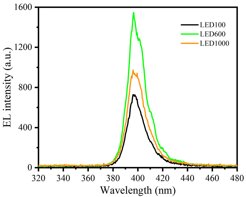
Figure 2: Electroluminescence spectra of 100 (LED100), 600 and 1000-second ramp LEDs under 100mA forward direct-current.
Temperature-dependent photoluminescence studies of the LED material suggested the presence of two types of recombination center: one with a low activation energy (14-15meV), and the other with a high activation energy (112-127meV). The ramp-up process seemed to have little effect on the low-energy recombination center type, but the 600-second ramp showed an increased activation energy (127meV) and reduced coupling coefficient, suggesting reduced density, for the higher energy center. Increasing the activation energy also reduces its impact for a given temperature. The 100- and 1000-second ramps resulted in activation energies for these centers at 112 and 116meV, respectively.
The SQW samples were used for atomic force microscopy (AFM) inspection. The 100-, 600-, and 1000-second ramp samples were found to have root-mean-square (rms) surface roughness values of 0.43, 0.31 and 0.37nm, respectively.
InGaN laser diodes InGaN LEDs InGaN GaN MOCVD
https://doi.org/10.1364/OE.449160
The author Mike Cooke is a freelance technology journalist who has worked in the semiconductor and advanced technology sectors since 1997.


