


News: LEDs
18 August 2022
Nanorod blue LED sidewall passivation
Researcher based in South Korea have developed a sol-gel sidewall passivation process for blue indium gallium nitride (InGaN) quantum well (QW) nanorod light-emitting diodes (nLEDs) with enhanced external quantum efficiency (EQE) over plasma-enhanced atomic layer deposition (ALD) [Mihyang Sheen et al, Nature, v608, p56, 2022].
Indeed, the team from Samsung Display, Korea Institute of Energy Technology (KENTECH), Pusan National University, and Samsung Electronics, claims that “the fabricated nLEDs showed an EQE of 20.2±0.6%, the highest EQE value ever reported for the LED in the nanoscale”; and that the value “is higher than the best EQE value of the μLED structure even at a larger size.”
The researcher believe that their work will accelerate the implementation of nLEDs in next-generation displays. Other potential benefits could be seen in solid-state lighting, optical data communication and photonic deployments, along with high-pixel-density display applications such as augmented/extended reality, which can be difficult to realize with liquid crystal technology.
Sidewall passivation becomes increasingly critical as device dimensions reduce since the surface area/volume ratio increases. Without suitable passivation, the EQE decreases through non-radiative electron-hole recombination at sidewall defects.
The material used for the nLEDs consisted of 8x(InGaN/GaN) multiple quantum wells (MQWs) between p- and n-GaN layers grown on 4-inch c-plane sapphire using metal-organic chemical vapor deposition (MOCVD). The structure also included a top layer of indium tin oxide (ITO) transparent conductor.
The 600nm-diameter nanorod structures were fabricated using nanoimprint lithography, inductively coupled plasma etch, and potassium hydroxide wet etch to remove surface damage. The wet etch also transforms the trapezoidal profile of the dry etched nanocolumn, giving more vertical sidewalls (Figure 1).
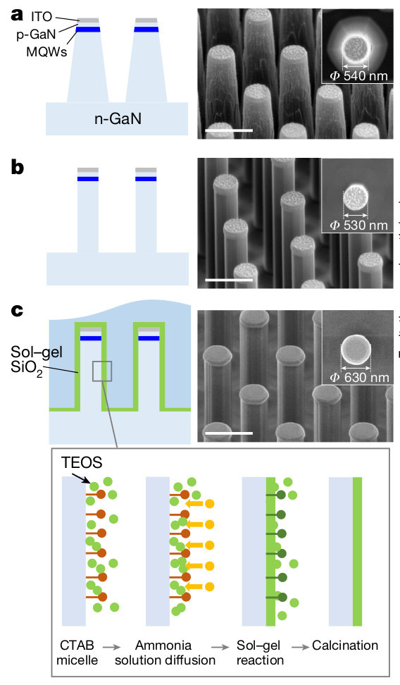
Figure 1: Schematics and corresponding scanning electron microscopy images of nLEDs fabricated by means of conventional top-down processing methods. Dry etching (a), wet etching (b) and deposition of SiO2 surface passivation layer by means of sol-gel method (c). Scale bars, 1μm. Inset: schematic of sol–gel reaction on GaN LED nanorod. Scale bars, 500nm (left) and 200nm (right).
The sidewall insulation consisted of two layers designed to meet the needs of display products for high efficiency, good reliability and processability. The inner passivation layer was 60nm silicon dioxide (SiO2); the outer etch-stop layer was 20nm aluminium oxide (Al2O3). These materials were chosen for their high transparency, low leakage current and high bandgap energy.
The researchers were keen to minimize added surface damage so they developed the low-temperature sol-gel method to apply the inner passivation. “Performing the sol–gel process at room temperature could minimize the atomic reaction between the GaN surface and the SiO2 layer and enhance the optical properties of the nanorods by passivating the dangling bonds,” the team writes.
The sol-gel process began with the nanorod wafer being dipped into an ethanol/deionized water solution to which was added cetyltrimethylammonium bromide (CTAB), forming micelles, and then an ammonia solution and the tetraethyl orthosilicate (TEOS) precursor for the SiO2 passivation. The sol-gel reaction saturated at around 23nm thickness. The full 60nm thickness was achieved by repeating the process.
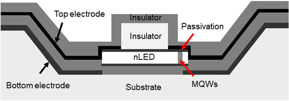
Figure 2: Schematic diagram of the nLED pixel structure.
One disadvantage of the sol-gel technique is the tendency toward by-product residue. The researchers tackled this by baking the sol–gel SiO2 film with the aim of good reliability through completing the reaction and eliminating reaction residues. The team reports that it is working on process optimization.
The use of sol-gel SiO2 deposition on the nanorods was found to enhance blue photoluminescence (PL) by ~13x over rods with the SiO2 applied using more conventional plasma-enhanced ALD. Also, the PL decay lifetime increased to 101.4ns, compared with 24.2ns for ALD passivation. The longer lifetime indicates more electron-hole recombination into photons as opposed to non-radiative routes.
The nanorod nLEDs were separated from the growth wafer using a diamond cutter and dispersed in solution for inkjet printing into pixel structures. The nanorods were aligned horizontally between two bottom electrodes using a dielectrophoretic force. Transparent top electrodes provided electrical biasing. The resulting pixel structures contained an average of 6 and 9 nanorods for the ALD and sol-gel passivation, respectively.
The researcher estimated the light extraction efficiency of the pixel structure at 25%, using finite-difference time-domain simulations. External quantum efficiency (EQE) measurements on 60-pixel arrays gave peak values of ~20% for the sol-gel nanorods and ~9% for the ALD passivation (Figure 3). Using the estimate for the light extraction efficiency, the corresponding internal quantum efficiencies (IQEs) were estimated at 81% and 36% for sol-gel and ALD passivation, respectively.
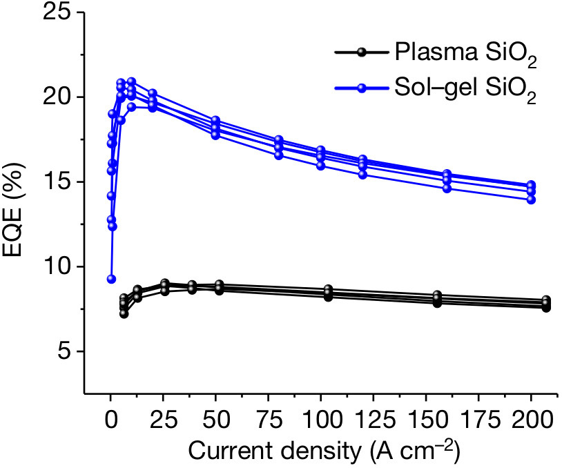
Figure 3: EQE versus current density for nLEDs.
The team deployed a wide range of material analysis techniques, such as photoluminescence (PL), electroluminescence (EL), cathodoluminescence (CL) and electron energy-loss spectroscopy (EELS) to track down the problems with the plasma-enhanced ALD passivation, concluding that “the VGa–ON–2H complex is the dominant defect generated in the sidewalls of the nanorods during the plasma-enhanced ALD SiO2 passivation, wherein a hydrogen-containing precursor is used.”
The plasma-enhanced ALD process also induces amorphization at the InGaN quantum well surfaces and creates point defects on the sidewalls of the GaN nanorods. These factors increases the Shockley-Read-Hall (SRH) electron-hole recombination mechanism through non-radiative recombination centers (NRCs) on the sidewalls of the InGaN QWs.
By contrast, “the sol–gel process provides effective passivation for the GaN surfaces because the SiO2 nanoparticles are adsorbed on the GaN surface after the sol–gel reaction,” the team explains, adding: “Thus, the atomic interaction with the GaN surface is minimized and only dangling bonds of the surfaces are passivated, resulting in a low leakage current, decreased NRC regions and high EQE.”


