


News: LEDs
25 August 2022
MOCVD Ohmic InGaN tunnel junction growth
North Carolina State University (NCSU) in the USA has reported progress in creating metal-organic chemical vapor deposition (MOCVD) indium gallium nitride (InGaN) tunnel junctions (TJs) with Ohmic conduction in the forward and reverse directions [B. G. Hagar et al, Appl. Phys. Lett., p121, p052104,2022]. The team comments : “We are not aware of any previous MOCVD-grown III-nitride TJs that display linear conduction in both forward and reverse biases.” While better TJ behavior is seen in molecular beam epitaxy structures, MOCVD is preferred in manufacturing.
Tunnel junctions have been proposed as solutions to various problems of III-nitride (and other) semiconductor devices such as multi-color light-emitting diode (LED) and multi-junction solar cell (MJSC) structures.
The NCSU team suggests that its achievement could be due mainly to the combination of three factors: a constant magnesium (Mg) concentration across the p/n layers allowed abrupt electron and hole concentrations at the junction interface; a constant Mg concentration reduced Mg diffusion, avoiding smudging of the junction; and Mg doping on the n side of the TJ created deep levels within the bandgap that enhances tunneling under forward-biased conditions.
The researchers explain the last factor: “Mg in GaN forms two levels within the bandgap: the Mg acceptor level is about 180–200meV above the valence band while another deep donor level exists at around 400–440meV below the conduction band. This deep donor level has been attributed to a Mg and nitrogen vacancy complex (Mg-VN). The transition between those two levels is responsible for the blue band emission, around 2.8eV, that is typically observed in the heavily doped p-GaN film.”
The same sort of behavior, or even better, is expected in InGaN. Generally, the hole concentration in p-InGaN is higher than for p-GaN doped with the same concentration of Mg. Thus, the researchers found that they did not need the very high Mg concentrations used by others (~1020/cm3), which can lead to pyramid defects. The NCSU Mg doping level was in the low-to-mid 1019/cm3 range.
Designing InGaN TJ structures with constant Mg doping avoids particular problems of MOCVD growth such as a delay in incorporation after the source starts to be supplied, and the memory effect where Mg continues to be incorporated after the supply is switched off. The memory effect may be due to temporary absorption of Mg on the reactor chamber wall. The delay and memory effects affect the abruptness of the doping profile. The n-type dopant (silicon) is not as subject to these effects. Sharp doping profiles are particularly critical in TJs where a very thin depletion layer is needed to increase tunneling probabilities.
The epitaxy was performed on commercial 5μm n-GaN on sapphire templates. The MOCVD was carried out in a home-made reactor with the substrate rotating under alternating streams of group-III and group-V precursor supplies (trimethyl metal-organics and ammonia, respectively) in hydrogen/nitrogen carriers. The silicon (Si) and magnesium (Mg) n- and p-type dopants came in the forms of silane (SiH4) and bis(cyclopentadienyl)magnesium (Cp2Mg), respectively.
The researchers made two sets of TJs: one set on GaN, the other on an InGaN ‘semi-bulk’ (SB) template layer (Figure 1). The latter was prepared by growing a series of thick InGaN layers separated by a thin high-temperature GaN layer, which aimed at backfilling V-pits generated during the relaxation of the InGaN. The indium content was controlled by the growth temperature during the InGaN MOCVD.
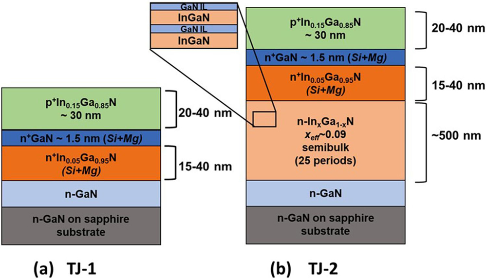
Figure 1: Schematic representation of (a) TJ-1 on GaN, and (b) TJ-2 on 25-period semi-bulk InGaN template. Period defined as InGaN and GaN interlayer (IL) pair.
The TJ consisted of n+-In0.05Ga0.95N and p+-In0.15Ga0.85N. The n+ layer used a Si+Mg co-doping strategy. The Mg flow was constant during the entirety of the TJ growth. Activation of the p-type layers was through 750°C annealing for 20 minutes in nitrogen. Test devices were fabricated with 400μmx400μm etch mesas and standard n- and p-type Ohmic contact metal electrodes.
The epitaxial structure resulted in strained TJs, which took advantage of the resulting piezoelectric field to bend the band structure, narrowing the depletion layer thickness.
The current-voltage behavior was non-rectifying and linear, i.e. ‘Ohmic’, in both structures (Figure 2). There was a wide spread in the results over at least 10 devices for each data point. The team suggests that this could be “due to a lack of a thick contacting layer as well as slight variations in the thickness and indium composition across the samples, especially for the p+ In0.15Ga0.85N film, which can be critical in the achieved hole concentrations.” The researchers add: “Such a lack of uniformity is expected in a home-built MOCVD system.”
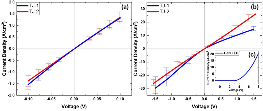
Figure 2: Current-voltage curves of TJ-1 (blue) and TJ-2 (red) at (a) low bias and (b) high bias with (c) inset showing MQW-based LED structure performance using identical mesa and metallization processes.
In the low-current region up to ±0.1V bias, the resistivity of both structures was around 8x10⁻²Ω-cm2. At higher bias, ±1.5V, the resistances deviated: the reverse-bias resistivities were in the range 5-6x10⁻²Ω-cm2; and the forward-bias values were 1x10⁻¹ and 6x10⁻²Ω-cm2 for TJ-1 and TJ-2, respectively.
The researchers point out that the forward-bias behavior is in contrast to previously reported results for MOCVD-grown TJs that had a backward diode behavior, rather than their TJs with similar behavior in both forward and reverse directions.
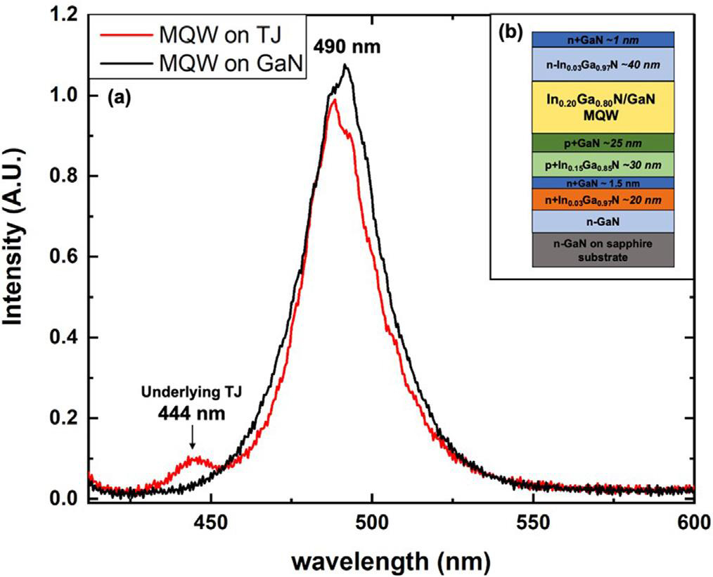
Figure 3: (a) Photoluminescence of MQW grown on TJ structure (red), compared to similar emitting MQW on GaN (black). (b) Schematic of MQW on TJ.
The team also report photoluminescence results from an LED structure with buried TJ on GaN, as in TJ-1, which allows inversion of the usual LED structure with the p-side below the n-side (Figure 3). Such an LED structure has been proposed as a way to access the desirable performance of N-polar devices which have the crystal orientation and strain-dependent electric fields reversed. One has to remember that buried p-GaN layers can be difficult to activate, since this requires expulsion of hydrogen from the layer. This is easier if the p-GaN is the top layer, dictating the usual structure. The NCSU team says it is working on fabricating buried TJ LEDs for future publication. The photoluminescence result showed comparable emission of the MQW-buried TJ with a conventional MQW-top p-GaN layer structure.
The author Mike Cooke is a freelance technology journalist who has worked in the semiconductor and advanced technology sectors since 1997.


