


News: LEDs
14 April 2022
High-Al-content p-AlGaN with 17.5meV activation energy
Peking University in China has improved the p-type behavior of high-aluminium-content aluminium gallium nitride (AlGaN) superlattices (SLs) and used the technique to improve the light output power and efficiency of 280nm-wavelength deep ultraviolet (DUV) light-emitting diodes (LEDs) [Jiaming Wang et al, Light: Science & Applications v11, p71, 2022].
The researchers comment: “It is expected that this study provides a solution for p-doping in Al-rich AlGaN, and it sheds light on solving the doping asymmetry issue in general for wide-gap semiconductors, especially for ternary and quaternary compound semiconductors.”
Normally p-type AlGaN has extermely low hole concentration and hole mobility due to the very high activation energy. This makes it difficult to create effective LEDs with holes combining with electrons from high-electron-concentration n-type AlGaN to produce photons. Asymmetry of doping ease is common in wide-bandgap semiconductors: n-type doping is much easier than p-type in III-nitrides and zinc oxide, while the reverse is the case for diamond (carbon).
Perodic interruption of the metal supply to the metal-organic chemical vapor deposition (MOCVD) growth process was used to create the AlGaN SLs. The metal-organic sources were trimethyl-Ga and -Al. The nitrogen precursor was ammonia (NH3).
The interruption results in a desorption phase where the material left behind exhibits a relative increase in aluminium content since Al atoms have a higher binding energy to N than Ga. Z-contrast scanning transmission electron microscope (STEM) analysis showed the higher-Al-content layer as consisting of 3 monolayers (MLs) of material, or about 0.75nm thickness. The researchers managed to achieve similar results for a range of base Al content AlGaN in the range 15-80% by varying the growth temperature in the range 1040-1160°C with desorption time in the range 20-100s.
Having understood the capability of the periodic interruption process, the team moved on to p-type doping with Mg. The base AlGaN material used an epitaxy process with 32s metal supply and 100s desorption, resulting in low (well)- and high (barrier)-Al-content layers of 7 and 3MLs, respectively. Energy-dispersive x-ray spectroscopy (EDS) mapping gave the respective Al contents of the layers at 46% and 63%, giving a 51% average. The doping occurred during the desorption phase of the growth using bis(cyclopentadienyl)Mg (Cp2Mg). This was found to enhance incorporation on metal sites in the lattice, since there was no Al or Ga competition.
The Mg concentration in the Al0.63Ga0.37N barrier layers was more than 1x10¹⁹/cm3. The measured hole concentration in the SL was 8.1x10¹⁸/cm3, claimed as “one of the highest values for Mg-doped Al-rich AlGaN reported to date”. Temperature-dependent studies suggested an effective activation energy for the Mg doping of 17.5meV, much lower than the usual >200meV values (Figure 1). It was also lower than the energy associated with 300K ‘room temperature’ of 26meV.
![Figure 1. Electrical properties of desorption-tailored Al-rich p-AlGaN SLs. (a) Temperature dependence of hole concentration. (b) Current-voltage (I-V) curves at room temperature of DUV-LED structures (inset) with p-AlGaN SLs period numbers of 25, 50 and 75, respectively. (c) I-V and corresponding dI/dV curves at 2K of DUV-LED structure with 25-period p-AlGaN SL. (d) Upward inclining of p-AlGaN SL energy (valence-band maximum, VBM) band profile along [0001] direction at equilibrium. (e) Resonant tunneling between E1 and adjacent E2 with flattened profile along [0001] direction under forward voltage. (f) Formation of minibands at even higher forward voltage.](2204-2-ST-news-p-AlGaN-SLs-and-DUV-LEDs-f1.jpg)
Figure 1. Electrical properties of desorption-tailored Al-rich p-AlGaN SLs. (a) Temperature dependence of hole concentration. (b) Current-voltage (I-V) curves at room temperature of DUV-LED structures (inset) with p-AlGaN SLs period numbers of 25, 50 and 75, respectively. (c) I-V and corresponding dI/dV curves at 2K of DUV-LED structure with 25-period p-AlGaN SL. (d) Upward inclining of p-AlGaN SL energy (valence-band maximum, VBM) band profile along [0001] direction at equilibrium. (e) Resonant tunneling between E1 and adjacent E2 with flattened profile along [0001] direction under forward voltage. (f) Formation of minibands at even higher forward voltage.
The researchers comment: “It is inferred that the reduction of the effective activation energy is attributed to the modulation of the hole activation path.” They continue: “Owing to the polarization-induced band bending in p-AlGaN SLs, the acceptor level in the barriers is quite close to the sub-band level in the wells, which then provides an energetically favorable path for the activation of Mg.”
In terms of current-voltage performance, the devices begin to turn on around 5V with a thinner 25-period SL structure delivering more current for a given voltage early on but, as the voltage reaches 9-11V, the thicker SLs have higher injection. The researchers explain the behavior by invoking band-flattening, resonant-tunneling, and miniband-formation effects as the voltage increases.
From analysis of the derivative behavior (dI/dV), the researchers estimate the series resistances of the three studied samples at 22.7, 11.9 and 3.8Ω for 25, 50 and 75 periods, respectively. The team write: “The inverse relationship between series resistance and SLs period (thickness) indicates a true miniband transport in SLs, where the miniband width plays a leading role.” With a higher numbers of layers, the miniband is expected to become wider, resulting in higher mobility and lower series resistance.
A very low-temperature (2K) study of the 25-period structure showed a peak-valley behavior above 9V in differential conductance (dI/dV), which the researchers label “negative differential resistance”, suggesting resonant tunneling. A p-GaN replacement of the AlGaN SL shows no such peak. The miniband forms when all the energy levels come into alignment. The eqilibrium V=0 band profile is tilted due to charge polarization effects from the partly ionic nature of the metal-nitrogen bonds.
The researchers used the p-AlGaN SLs on multiple quantum well (MQW) light-emitting regions to produce 280nm-wavelength DUV-LEDs (Figure 2).
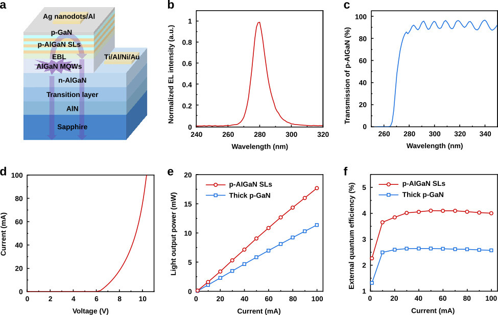
Figure 2. Performance of DUV-LEDs fabricated with desorption-tailored Al-rich p-AlGaN SLs. (a) Schematic. (b) Electroluminescence spectrum (at 100mA) of DUV-LEDs. (c) Transmission spectrum of desorption-tailored p-AlGaN SLs (without p-GaN contact layer). (d) I-V curve of DUV-LEDs with p-electrode of complex silver nanodots/Al. (e, f) Dependence of light output power and EQE on injection current for DUV-LEDs.
Using AlGaN rather than GaN for the p-contact could also be beneficial in terms of greater transparency to the target DUV light. The ~3.4eV bandgap of GaN corresponds to a photon wavelength around 365nm, meaning that wavelengths shorter than that (e.g. 280nm) are strongly absorbed by excitation of electrons from the valence band to the conduction band.
The researchers used a reflective p-electrode consisting of silver nanodots in aluminium on a thin 8nm p-GaN contact layer so that the light could be collected from the side of the sapphire substrate. The turn-on voltage was 6.2V. The devices were encapsulated in a hemispherical lens structure.
At 100mA injection current, the light output power reached 17.7mW, a 57% improvement on devices with a thick p-GaN contact layer. The external quantum efficiency (EQE) reached 4.1%.
The researchers comment: “Through comparative analysis, the enhancement of the light extracting efficiency (LEE) contributes about two-thirds of the performance improvement, while the rest is from the enhancement of the carrier injection efficiency (CIE).”
N-polar InGaN LEDs InGaN LEDs MOCVD
https://doi.org/10.1038/s41377-022-00753-4
The author Mike Cooke is a freelance technology journalist who has worked in the semiconductor and advanced technology sectors since 1997.


