


News: Suppliers
20 April 2022
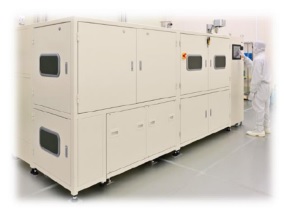
Nippon Sanso’s first Ga2O3 MOCVD system installed and qualified
Taiyo Nippon Sanso Corp (TNSC) of Tokyo, Japan has installed its first gallium oxide (Ga2O3) metal-organic chemical vapor deposition (MOCVD) system in the laboratory of professor Yoshinao Kumagai at the Tokyo University of Agriculture and Technology.
 Beta-phase gallium oxide (β-Ga2O3) is attracting attention as a semiconductor material for next-generation power (and energy-efficient) devices. In October 2020, TNSC and Tokyo University of Agriculture and Technology began joint research on β-Ga2O3 thin-film growth by MOCVD, and in March 2021 they announced the successful MOCVD growth of β-Ga2O3.
TNSC says that its newly designed Ga2O3 MOCVD system (Model FR2000-OX, with a process capability of 1x2-inch wafer) will make it possible to fabricate complex device structures and further stimulate R&D of these materials. Features include an MOCVD growth chamber for the high-purity and high-speed growth of oxides on β-Ga2O3 substrates to meet the needs of thick-film and alloy growth for research on high-performance electronic devices.
TNSC says that it will continue to enhance its Ga2O3 MOCVD technology to enable more energy-efficient semiconductor technology.


