


News: Microelectronics
28 April 2022
Gallium oxide on strontium titanate
Researchers based in USA have demonstrated successful epitaxial integration of β-polytype gallium oxide (β-Ga2O3) on a strontium titanate (SrTiO3 or STO) surface [Tobias Hadamek et al, J. Appl. Phys., v131, p145702, 2022]. The growth was demonstrated for STO in the form of either bulk material or a buffer layer on silicon (Si).
Ga2O3 is an ultra-wide-bandgap material with potential for high-power electronics and ultraviolet (UV) light detection. The material is transparent to visible light, offering solar-blind UV capability. The researchers also point to microwave switching and amplification as a possibility.
The ~5eV bandgap corresponds to a wavelength of 250nm in the deep UV range (<300nm) and UV-C (200-280nm), making it transparent to softer UV-A (315-400nm) and UV-B (280-315nm) electromagnetic radiation.
For high-power electronics, the high theoretical breakdown field of about 8MV/cm is extremely attractive, if it can be approached in practice.
The team from University of Texas at Austin, Arizona State University, and Staib Instruments Inc, comments: “The epitaxial integration of Ga2O3 with silicon serves as a template layer for subsequent fast deposition methods and could enable the fabrication of large-area wafers that, in turn, could advance Ga2O3-based technologies.”
The researchers see their epitaxial β-Ga2O3 on STO being used as a seed layer for further epitaxial growth. Particularly interesting is where STO is used as a buffer layer on silicon wafers.
Although bulk Ga2O3 is commercially available in wafers up to 4-inch diameter, silicon wafers can be as large as 12-inches (300mm). An STO buffer prevents silicon oxidation and reaction between Ga2O3 and Si during growth, which is a problem for direct Ga2O3 growth on silicon.
Another disadvantage of bulk Ga2O3 substrates is the low thermal conductivity (0.1–0.3W/cm-K), particularly for high-power systems where one expects significant Joule heating that needs to be dissipated effectively.
The researchers used plasma-assisted molecular beam epitaxy (PAMBE) on 10mm STO bulk and 2-inch STO-buffered silicon substrates. The growth temperature was 775°C at the silicon carbide heater coil, corresponding to a silicon substrate temperature of ~670°C. The STO was treated with oxygen plasma before the growth of Ga2O3. Before that, the surface was cleaned aand rinsed in de-ionized water, resulting in a TiO2-terminated surface.
The deposited material contained 5-10nm crystal grains of β-Ga2O3. “Small crystal grains result from the symmetry and the lattice mismatch between the film and the substrate,” the team explains.
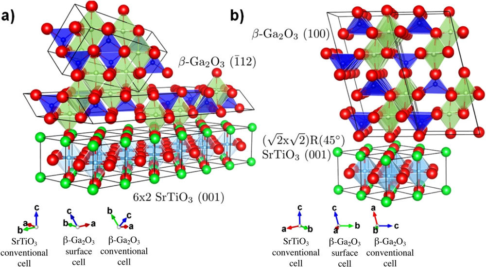
Figure 1: Lattice matching illustrated for (a) β-Ga2O3 (-112) and (b) (100) surface-oriented cells placed on top of STO (001).
The Ga2O3 was found to be crystalline as-grown, unlike with metal-organic chemical vapor deposition (MOCVD). There were two main grain orientations, according to x-ray diffraction (XRD) analysis: (100) and (-112) parallel to the (001) orientation of the STO (Figure 1). The team estimates the (100) volume fraction to be about three times that of (-112). Both orientations were found to also have four in-plane rotational domain variants.
![Figure 2: (a) Low-magnification TEM image of 20nm Ga2O3 film along [100] zone-axis of STO. (b) High-magnification TEM image. (c) Fast-Fourier-transform of image in (b); spots originating from Ga2O3 thin film are consistent with model obtained from XRD.](22044_arizona_f2.jpg)
Figure 2: (a) Low-magnification TEM image of 20nm Ga2O3 film along [100] zone-axis of STO. (b) High-magnification TEM image. (c) Fast-Fourier-transform of image in (b); spots originating from Ga2O3 thin film are consistent with model obtained from XRD.
These findings were also based on reflection-high-energy electron diffraction (RHEED), reflection electron-energy-loss spectroscopy (REELS), and transmission electron microscopy (TEM) - see Figure 2 - along with density functional calculations and other measurements.
Gallium oxide Strontium titanate UV PAMBE
https://doi.org/10.1063/5.0082859
The author Mike Cooke is a freelance technology journalist who has worked in the semiconductor and advanced technology sectors since 1997.


