


News: Markets
9 September 2021
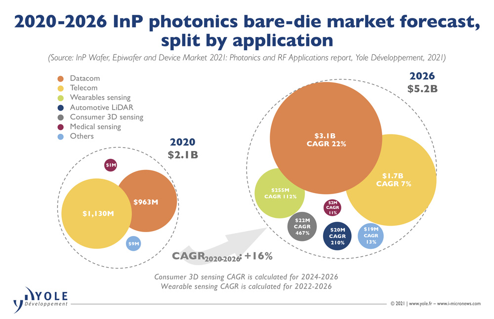
InP bare die market growing at 16% CAGR from $2.1bn in 2020 to $5.2bn in 2026, with datacom and telecom sectors growing at 22% and 7%
In its report ‘InP Wafer, Epiwafer and Device Market 2021: Photonics and RF Applications’, Yole Développement estimates that the market for indium phosphide (InP) bare die is growing at a compound annual growth rate (CAGR) of 16%, from $2.1bn in 2020 to $5.2bn in 2026.
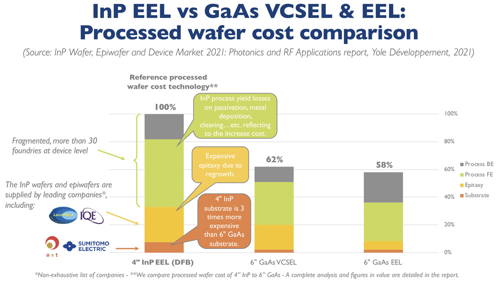
As an indispensable building block for high-speed and long-range optical transceivers, InP laser diodes remain the best choice for telecom and datacom photonic applications, says Yole. However, following the outbreak of the COVID-19 pandemic and the US-China trade tensions, telecom infrastructure deployment was disrupted (with many laser and photonics companies losing big customers), resulting in a slight slowdown in the InP market in 2020. However, the requirement for more data transfer at higher speed in datacoms is increasing, with technology migrating to single InP lasers targeting state-of-the-art 100Gbps output, making them preferable in 400Gbps and 800Gbps transceivers.
Driven by high-volume adoption of high-data-rate lasers, the bare die market for datacom applications reached about $963m in 2020, and is estimated to be growing at a CAGR of 22% to $3.1bn in 2026.
Meanwhile, due to 5G deployment, the cyclical InP telecom market should continue to grow steadily at a CAGR of 7%, from $1.1bn in 2020 to $1.7bn in 2026, reckons Yole.
Yole expects initial slight market penetration of InP in 2022 in wearables, followed by a significant increase at a CAGR of 112% to $255m in 2026.
“For light detection and ranging (LiDAR) applications, InP could be promising, enabling eye safety at higher wavelengths,” says Ahmed Ben Slimane PhD, technology & market analyst, Compound Semiconductors and Emerging Substrates, at Yole. “Leading companies such as Volvo, ZF, Continental, Daimler etc are interested in adopting InP-based LiDAR,” he adds. The automotive LiDAR sector is hence forecasted to grow at a CAGR of 210% to $20m in 2026.
For smartphones, organic light-emitting diode (OLED) displays are transparent at wavelengths in the range of 13xxnm to 15xxnm. Original equipment manufacturers (OEMs) interested in removing the camera notch on mobile phone screens and integrating the 3D sensing modules under OLED displays are considering moving to InP edge-emitting lasers (EELs), replacing the existing gallium arsenide (GaAs) vertical-cavity surface-emitting lasers (VCSELs). Even though this trend is currently in an early R&D phase (with process yields still low, hampering the economy-of-scale), Yole sees strong interest from several players, such as ams, Infineon Technologies, STMicroelectronics, and several laser manufacturers and sensor players. The consumer 3D sensing sector is hence forecasted to grow at a CAGR of 467% to $22m in 2026.
Market players in supply chain
As a dynamic market with lots of opportunities for both legacy players and new entrants, Yole notes that the InP market is fragmented, with numerous companies, especially at the device level.
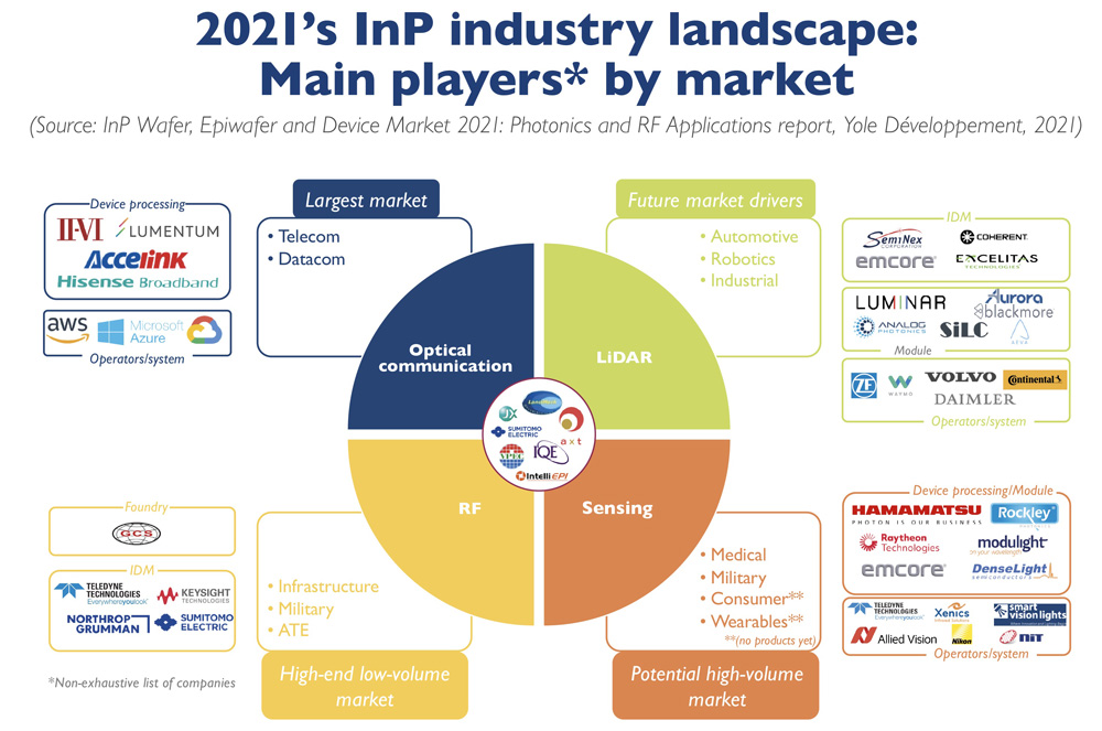
“Two American players are leading the InP market: II-VI and Lumentum,” says Ahmed Ben Slimane. “Both have increased their market share and strengthened their position thanks to strategic mergers and acquisitions. Indeed, II-VI acquired Finisar in 2019 and Lumentum acquired Oclaro in 2018.”
II-VI and Lumentum both have vertically integrated business models: they generate revenues at bare die, device, and module levels. II-VI also offers epiwafer products. Their combined bare die market share is about 30%.
Facing II-VI and Lumentum, Yole identifies major Chinese players such as Hisense and Accelink. Both these companies are in the global top five and are increasing their market share step by step. The two Chinese firms are taking advantage of the US-China trade tensions and China investing heavily in optical infrastructure (with the massive deployment of 5G transceiver in Asia), says Yole.
Sensing applications targeting the mass consumer and automotive markets are attracting new players. Yole has hence identified several types of player interested in entering this market:
- Vertically integrated InP players with the know-how and an already established structure, as they can easily switch to sensing applications as soon as the market becomes bigger. II-VI and Lumentum are part of this segment.
- GaAs players with foundry capabilities (e.g. ams and Trumpf) could leverage the existing GaAs tools to switch to similar InP processes.
- Emerging foundries or companies already working on InP-based solutions.
“In the last category, we witnessed an increase in private investments and SPACs [special-purpose acquisition companies] in the last year,” notes Poshun Chiu, technology & market analyst, Compound Semiconductors & Emerging Materials. “These include, in Q4-2020, Luminar raised $590m and went public, then acquired OptoGration; in Q2-2021, Aeva went public with an initial valuation of $1.7bn; and in Q2-2021, Rockley Photonics announced its intention to go public at an initial valuation of $1.2bn with an Apple-supported project for smartwatches,” he adds.
Yole notes that the InP epiwafer market continues to be dominated by LandMark (with over 60% of the open epiwafer market share). Sumitomo and AXT continue to lead the substrate market (with combined market share of more than 75%).


