


News: Optoelectronics
12 November 2021
Metal modulated AlGaN superlattices
Georgia Institute of Technology (GaTech) in the USA has been exploring the use of metal modulated epitaxy (MME) to produce aluminium gallium nitride (AlGaN) self-assembled superlattices (SASLs) [Zachary Engel et al, J. Appl. Phys., v130, p165304, 2021].
AlGaN superlattices have a wide potential in III-nitride device structures from providing strain management and dislocation filtering in buffer layers through to electroluminescence in multiple quantum wells (MQW) and distributed Bragg reflectors (DBRs) for creating laser cavities. In terms of systems and so on, these feature could enable production of better power electronics and light-emitting diodes/lasers.
The bandgap range (3.4-6.1eV, GaN-AlN) of AlGaN alloys ranges from the near-ultraviolet to deep-ultraviolet: 365nm to 200nm wavelength. Light around 250nm has a strong virus/bacteria-killing effect through DNA disruption.
GaTech’s MME method avoids growth interruptions where the unintentional accumulation of contaminants at interfaces can lead to loss of optical emission and/or structural defects.
The MME technique was applied using molecular beam epitaxy (MBE) on 1cmx1cm AlN-on-sapphire templates, produced by halide vapor phase epitaxy (HVPE). The researchers sputtered 2μm of tantalum on the backside of the templates with a view to improving thermal uniformity during the MME/MBE process.
After an initial MBE AlN buffer layer, the MME process consisted of supplying the group-III metals with a 1.3 III/V ratio, and shuttering the metal supply with an open/close cycle of up to 21/11s. The substrate temperature was 725°C. The process was monitored using reflection high energy electron diffraction (RHEED).
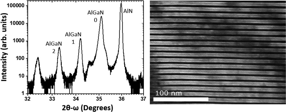
Figure 1: X-ray diffraction 2θ-ω scan (left) of SASL and cross-sectional transmission electron micrograph (right) of sample grown with 1.3 III/V, 14s open-shutter, 2.4μm/h instantaneous growth rate.
The SASL growth effect from MME (Figure 1) arises from the different compositions of the AlGaN when the shutter is open and closed, due to different chemical strengths of the Ga–N and Al–N bonds. During the open part of the cycle Al/Ga metal is supplied to the growth front along with nitrogen plasma. When the metal is cut off, metal on the surface of the sample continues to consume the nitrogen, which continues to be supplied during the closed phase, producing a different composition AlGaN. The periods of the SASLs varied with the shutter-open time: 4.6nm, 6.4nm and 9.1nm for metal doses of 10s, 14s and 20s, respectively (Table 1).
Table 1: SASL parametes extracted from x-ray diffraction data, using simulations. Material with 3s open time was single-phase Al0.55Ga0.45N.
| Sample ID | Shutter open time (s) | Average well Al% | Well thickness (nm) | Average barrier Al% | Barrier thickness (nm) | SL period (nm) | Twell/Tbarrier |
| D1 | 3 | N/A | N/A | N/A | N/A | N/A | N/A |
| D2 | 10 | 31 | 1 | 66 | 3.5 | 4.5 | 0.29 |
| D3 | 14 | 18 | 1.5 | 70 | 4.9 | 6.4 | 0.31 |
| D4 | 20 | 8 | 2.1 | 67 | 7 | 9.1 | 0.3 |
The ratio of lower (well) to higher (barrier) Al composition material thickness was relatively constant at around 30%. The researchers posit that the 30% arises from the III/V ratio being 1.3, 30% being the excess metal during the open phase, which is then consumed during the closed phase. This suggests that the barrier part is the material grown during the open part of the cycle.
The team comments: “We note that the compositions of the well and barrier are different because Al is preferentially grown into the film compared to Ga because the Al–N bond strength in AlGaN is stronger than the Ga–N bond strength in AlGaN. Thus, the metal remaining on the surface after the barrier is grown (at the end of the shutter open time) is Ga-rich, leading to a lower-Al-composition well...”
The researchers also note that the barrier Al content varies by only 4 percentage points, while the well content ranges from 8% to 31%. They suggest that this is a result of the higher-Al-content material being a closer lattice match to the AlN template. This is another factor favoring Al incorporation during the open-shutter time.
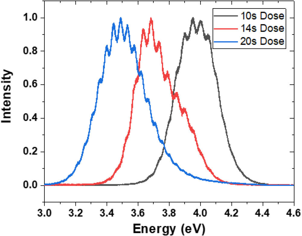
Figure 2: Room-temperature PL spectra of AlGaN SASL structures grown with 10s, 14s and 20s dose showing control of emission energy.
Photoluminescence (PL) measurements (Figure 2) confirm the shift in well composition with the peak varying from ~4eV (31% Al well) photon energy down to 3.5eV (8% Al). The mid- 18% Al structure had a peak ~3.7eV. All PL spectra show oscillations from Fabry-Perot interference/reflections from the 4-5μm cavity structure of the samples. The linewidth is fairly broad due to the large numbers of wells: 44, 63 and 88 wells for 20s, 14s and 10s doses, respectively.
Increasing the III/V ratio to 1.8 resulted in a well/barrier ratio of 80%. A structure grown with 14s open-shutter time had 4nm Al0.4Ga0.6N wells and 5nm Al0.7Ga0.3N barriers. The barrier composition matched that with 1.3 III/V. The Al composition in the well was higher than for 1.3 III/V, and the Ga had to be consumed over a thicker well.
The flux of the precursors was also varied. The instantaneous growth rate was increased from 1.3μm/h to 2.8 with 14s shutter-open and 1.3 III/V. The structure consisted of 3.3/11.1nm Al0.14Ga0.86N/Al0.67Ga0.33N wells/barriers. The higher growth rate naturally resulted in thicker structures: 910nm, compared with 400. The higher growth rate was also found to result in a more coherent SASL, according to the x-ray diffraction (XRD) data.
The instantaneous growth rate was defined as “(the deposited material thickness per cycle)/(the cycle time minus the dead time per cycle)”. The dead time was the amount of time the RHEED monitoring indicated that no growth was taking place in the shutter-closed part of the cycle.
The researchers comment: “We can specify any arbitrary SASL geometry by controlling III/V ratio, total metal dose, and instantaneous growth rate.”
Metal modulated epitaxy Self-assembled superlattices AlGaN GaN AlN MBE HVPE
https://doi.org/10.1063/5.0069534
The author Mike Cooke is a freelance technology journalist who has worked in the semiconductor and advanced technology sectors since 1997.


