


News: LEDs
20 August 2021
Gallium oxide white LED prospects
Saga University in Japan has reported work towards white light-emitting diodes (WLEDs) based on rare-earth (RE)-doped gallium oxide (Ga2O3) [Yafei Huang et al, Appl. Phys. Lett., v119, p062107, 2021].
The researchers adopted a vertical integration strategy with Ga2O3 layers doped with thulium (Tm), europium (Eu) and erbium (Er) grown on top of each other. The team comments that “films grown by lateral integration are deposited side-by-side, while the co-doping of multiple rare earth elements into the same host will unavoidably degrade the crystal quality and, thus, induce undesirable threshold voltage and luminous efficiency.” The vertical strategy leads to more compact devices without compromising crystal quality.
The team adds: “On the other hand, compared with phosphor-assisted WLEDs, direct white light emissions are achieved from single-material-based LEDs in this work without using additional red, blue or green phosphors, which can greatly reduce the energy re-absorption effect between different phosphors.” Such energy re-absorption would naturally impact power efficiency.
The researchers also see the phosphor-free approach based on single-material-based WLEDs with direct primary color mixing as more conducive to displays based on smaller-pixel micro-LEDs. Although rare-earth doping has been tried in gallium nitride and zinc oxide devices, there are problems such as needing high voltages (~100V) or poor color balance due to spectral gaps.
The Saga team sees β-Ga2O3 as “an ideal host for rare-earth ions benefiting from its ultrawide bandgap (4.9eV), which is advantageous to improve the thermal stability and luminous ability of rare-earth dopants at room temperature”. According to the researchers, at present, “there are no reports available related to full-color (white) LEDs based on rare-earth-doped Ga2O3.”
The doped Ga2O3 layers were deposited on p-type gallium arsenide, p-GaAs (111), using alternate-target pulsed laser deposition (PLD) at 500°C. The Ga2O3 targets were variously doped with rare-earth oxides: 1wt.% Tm2O3, 1wt.% Eu2O3 and 5wt.% Er2O3. The laser light came from a krypton fluoride (KrF) excimer laser emitting deep-ultraviolet light at 248nm wavelength. The PLD was carried out in an oxygen atmosphere at 0.1Pa pressure.
The samples consisted of 150-periods of the sequence of the three types of Ga2O3 doping (Figure 1). The growth process lasted 150 minutes. Material analysis suggested that the atomic concentrations for the doped layers were 0.3% Tm, 0.5% Eu and 2.3% Er.
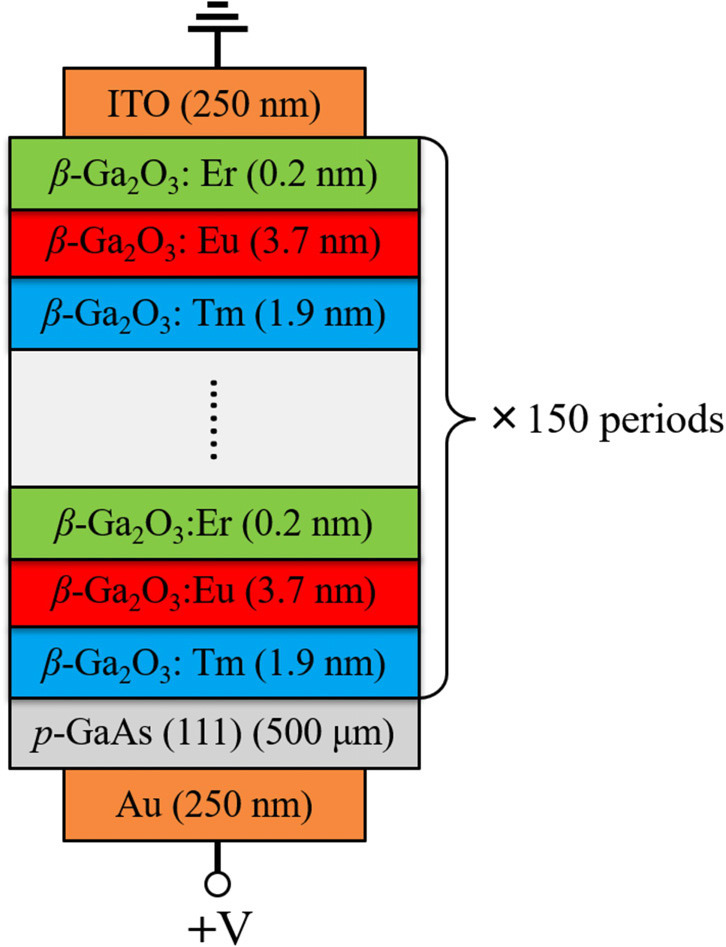
Figure 1: Schematic structure of LED-A based on Ga2O3:(Tm+Eu+Er)/GaAs heterojunction.
The LEDs featured an indium tin oxide (ITO) transparent conductor n-electrode and gold (Au) p-electrode. The ITO was applied with direct-current sputtering; the gold with electon-beam evaporation.
Atomic force microscopy showed a sample surface “filled with uniformly distributed grain-like structures” with a root-mean-square roughness of 10nm.
When subjected to a forward voltage of more than 8.8V, the current begins to increase rapidly. The researchers also note that the electroluminescence (EL) is only observed under forward bias, suggesting that “simultaneously injected electrons and holes are indispensable for the EL”. The researchers associate the emitted light with 4f transitions from the Eu3+, Er3+, and Tm3+ ions (Figure 2).
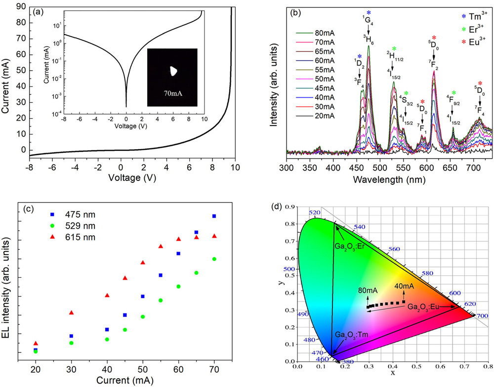
Figure 2: (a) Current-voltage characteristics curve of LED-A. Inset: semi-log characteristics and digital photograph of LED-A at 70mA. (b) EL spectra under different operating currents. (c) EL intensities of emissions at 475, 529, and 615nm as function of injection current. (d) CIE chromaticity coordinates under different currents.
The various peaks associated with the different ions were: 461 and 475nm with Tm3+; 529, 550, and 656nm with Er3+; 590, 615, and 712nm with Eu3+. Although the emissions somewhat overlap, the Tm ones are mainly in the blue range, Er green, and Eu red. The combination gives white light.
The researchers explain: “Due to the existence of oxygen vacancy defects in the film, the simultaneous red, green, and blue emissions are supposed to be triggered by the defect-assisted energy transfer from the Ga2O3 host to RE3+ (Eu3+, Er3+, and Tm3+) ions.”
On the basis of previous reports, the researchers expect the emission to be relatively independent of the temperature environment since the complete outer 5s and 5p orbitals shield the 4f shell from such influence.
The positions of the peaks were found to vary little with changing current injection. However, the strength of the emissions did vary, with the balance shifting from red to green and blue as the current increases. The color content of the main device reported, LED-A, shifted from pink to white with injections from 40mA to 80mA. The correlated color temperature (CCT) varied from 2370K to 7592K, respectively, a shift from a warm to cold tone.
The team reports: “For instance, the emitted light at 55mA locates at a warm-white point with CIE coordinates of (0.3739, 0.3410) and CCT of 3926K, which meets the requirements for indoor lighting applications.” The researchers also see 65mA as providing “superior” CIE coordinates, (0.3329, 0.3335), but 5479K CCT, suitable for indoor/outdoor cold-white illumination.
Table 1: Thicknesses of doped Ga2O3 layers.
Sample |
Ga2O3:Tm | Ga2O3:Eu | Ga2O3:Er |
| LED-A | 1.9nm | 3.7nm | 0.2nm |
| LED-a | 2.0nm | 3.2nm | 0.4nm |
| LED-b | 2.6nm | 1.9nm | 0.4nm |
| LED-c | 1.0nm | 5.1nm | 0.4nm |
| LED-d | 1.3nm | 2.6nm | 1.4nm |
The color balance was also varied in hardware, with the researchers producing four other device structures with different layer thicknesses of the various components (Table 1). These resulted in different color balance behavior (Figure 3).
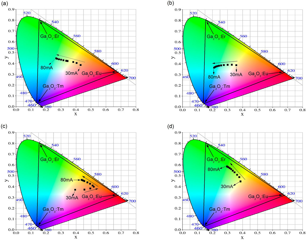
Figure 3: CIE chromaticity diagrams for (a) LED-a, (b) LED-b, (c) LED-c, and (d) LED-d under different operating currents.
White LEDs RE-doped gallium oxide PLD p-GaAs
https://doi.org/10.1063/5.0060066
The author Mike Cooke is a freelance technology journalist who has worked in the semiconductor and advanced technology sectors since 1997.


