


News: Microelectronics
22 April 2021
Diamond for Ga2O3 thermal management
Researchers based in the USA claim “the first significant step towards device-level thermal management of β-Ga2O3 electronic devices” with the development of a polycrystalline diamond deposition process [Mohamadali Malakoutian et al, Appl. Phys. Express, vol14, p055502, 2021].
Gallium oxide (Ga2O3) is a promising material for high-voltage and high-power-density applications due to its wide bandgap of 4.8eV and resultant resistance to breakdown under large electric fields up to 8MV/cm. Further, high-quality low-cost melt-grown Ga2O3 wafers are commercially available.
However, thermal management is a critical consideration for high-power devices, and unfortunately Ga2O3 has a relatively low and anisotropic thermal conductivity in the 11-27W/m-K range. In recent years, thermally conductive diamond layers have been proposed for thermal management across a wide range of electronics applications.
The team from Stanford University, Pennsylvania State University, Georgia Institute of Technology, and University of California Davis, used (-201) β-Ga2O3 substrates from Sojitz Machinery Corp in Japan. The substrates were tin-doped.
The 5-10nm-diameter diamond nanoparticles were supplied by Adamas Nanotechnologies in the USA, suspended in deionized water and dimethyl sulfoxide (DMSO). The colloidal dispersions had various zeta potentials, both positive and negative. Three seeding processes were tried: ultrasonication, drop, and polymer-assisted.
The main diamond growth was by microwave plasma chemical vapor deposition (CVD). The carbon source was methane (CH4). The growth temperature was between 500°C and 700°C.
The researchers found that ultrasonication seeding was not viable for the subsequent CVD process because the seed deposition resulted in bare Ga2O3 patches, which were decomposed by the hydrogen plasma in the CVD reaction chamber. This resulted in non-contiguous diamond layers.
Drop-seeding used a nanoparticle suspension diluted with DMSO. This enabled a contiguous diamond layer to be grown by CVD. However, the seeding layer was very thick, giving a non-uniform CVD diamond layer. Further, the diamond tended to delaminate if thicker than 200nm. This was attributed to a larger coefficient of thermal expansion (CTE) mismatch between Ga2O3 and diamond.
Polymer-assisted seeding consisted in coating the Ga2O3 surface with poly-diallyldimethylammonium chloride (PDDAC) beforehand. This created a negative potential surface, which attracted diamond nanoparticles with positive zeta potential. The resulting seed layer consisted of a nanoparticle monolayer with a density of more than 1012/cm2.
CVD growth with a single polymer-assisted seed layer was found to have insufficient coverage to protect the Ga2O3 from hydrogen-plasma attack, as before. Therefore, the researchers modified the method to give three nanoparticle monolayers. Even so, the CVD diamond was non-uniform.
Finally, the researchers applied a thin silicon dioxide (SiO2) layer to the Ga2O3 through plasma-enhanced CVD. SiO2 is less subject to decomposition under hydrogen plasma than Ga2O3. This allowed the use of a single monolayer of polymer-assisted nanoparticles to be used as seed.
The team describes the resultant uniformity of the diamond film as “excellent” (Figure 1). The layer thicknesses were 19nm SiO2 and 260nm diamond. A diamond layer grown on 100nm SiO2 reached 930nm thickness – the average grain size was ~400nm. The grain size for the thinner film was ~130nm.
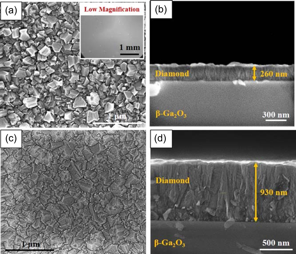
Figure 1: Scanning electron micrographs of polycrystalline diamond films grown on SiO2/Ga2O3: (a) and (b) ~260nm diamond on 19nm SiO2. Inset shows uniform growth on larger area of surface; (c) and (d) ~930nm diamond on 100nm SiO2.
The team comments: “Adding a dielectric layer prevents substrate etching and improves diamond adhesion onto the surface. Also, thicker diamond growth becomes possible due to reduction in the diamond film residual stress by lowering the CTE mismatch between the diamond and the dielectric layers.”
Time- and frequency-domain thermoreflectance (TDTR and FDTR) were used to characterize the thermal conductivity and boundary resistance. Thermoreflectance involves detection of acoustic waves generated by pulsed laser radiation. The resulting response is analyzed to extract the thermal properties of material structures. For example, TDTR studies with an 82nm gold layer as transducer between 1.2MHz laser pulses and the acoustic waves were used to extract thermal conductivities. FDTR across the range 10kHz-20MHz enabled the boundary resistance to be derived, using the TDTR thermal conductivities as part of the input. These FDTR resistances were found to be more precise than estimates derived using just TDTR.
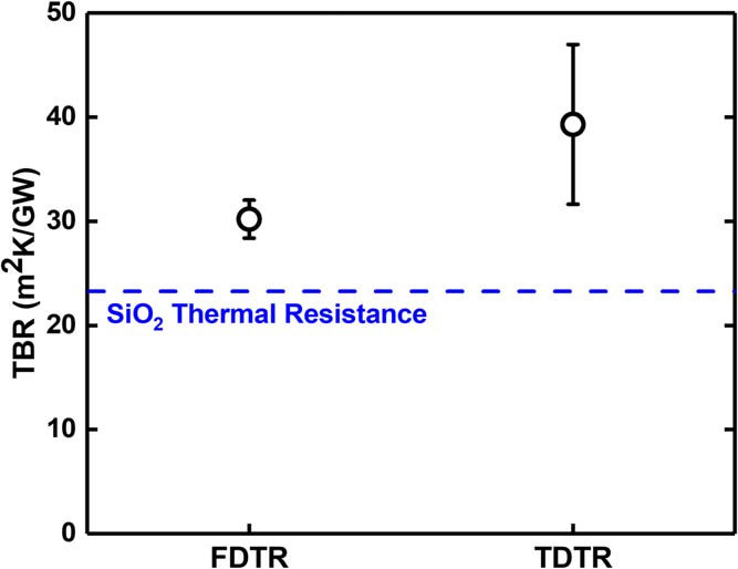
Figure 2: Effective diamond/β-Ga2O3 TBR measured by TDTR and FDTR methods. Dashed line shows estimated contribution from 19nm SiO2 interlayer.
The direction-averaged thermal conductivity of the ~260nm diamond film was estimated at ~110W/m-K. The thermal boundary resistance (TBR) was derived using both TDTR and FDTR (Figure 2). The SiO2 layer accounted for about three-quarters of the thermal boundary resistance of ~30m2K/GW. The researchers add: “The rest of the TBR is thought to mainly originate from the diamond nucleation region defects and the interface roughness.”
https://doi.org/10.35848/1882-0786/abf4f1
www.sojitz-mac.com/en/division/mobility_1
The author Mike Cooke is a freelance technology journalist who has worked in the semiconductor and advanced technology sectors since 1997.


