


News: Microelectronics
8 April 2021
Routes to stacked III-V RF on silicon logic
Researchers based in Korea claim the highest cut-off and maximum oscillation frequencies reported for RF transistors with gate lengths longer than 100nm aimed at monolithic 3D (M3D) integration with silicon circuitry [Jaeyong Jeong et al, IEEE Transactions on Electron Devices, published online 23 March 2021].
The team from KAIST (formerly the Korea Advanced Institute of Science and Technology), Korea Advanced Nano Fab Center (KANC) and Gwangju Institute of Science and Technology ensured that the fabrication processing temperature was below 250°C with a view “to minimize the thermal budget for the bottom interconnects and bottom Si devices”.
The researchers see the combination of high-speed III-V materials with silicon circuitry as providing a route to mixed-signal radio-frequency analog and digital logic capabilities in the millimeter-wavelength range.
The III-V material was grown on indium phosphide (InP) substrates by molecular beam epitaxy (MBE) – see Figure 1. The channel region was an indium arsenide (InAs) quantum well in indium gallium arsenide (InGaAs) barriers. This resulted in 25μm gate-length (LG) ‘long-channel’ transistors achieving an effective mobility of 7950cm2/V-s, compared with 5550cm2/V-s for similar transistors using an InGaAs channel.
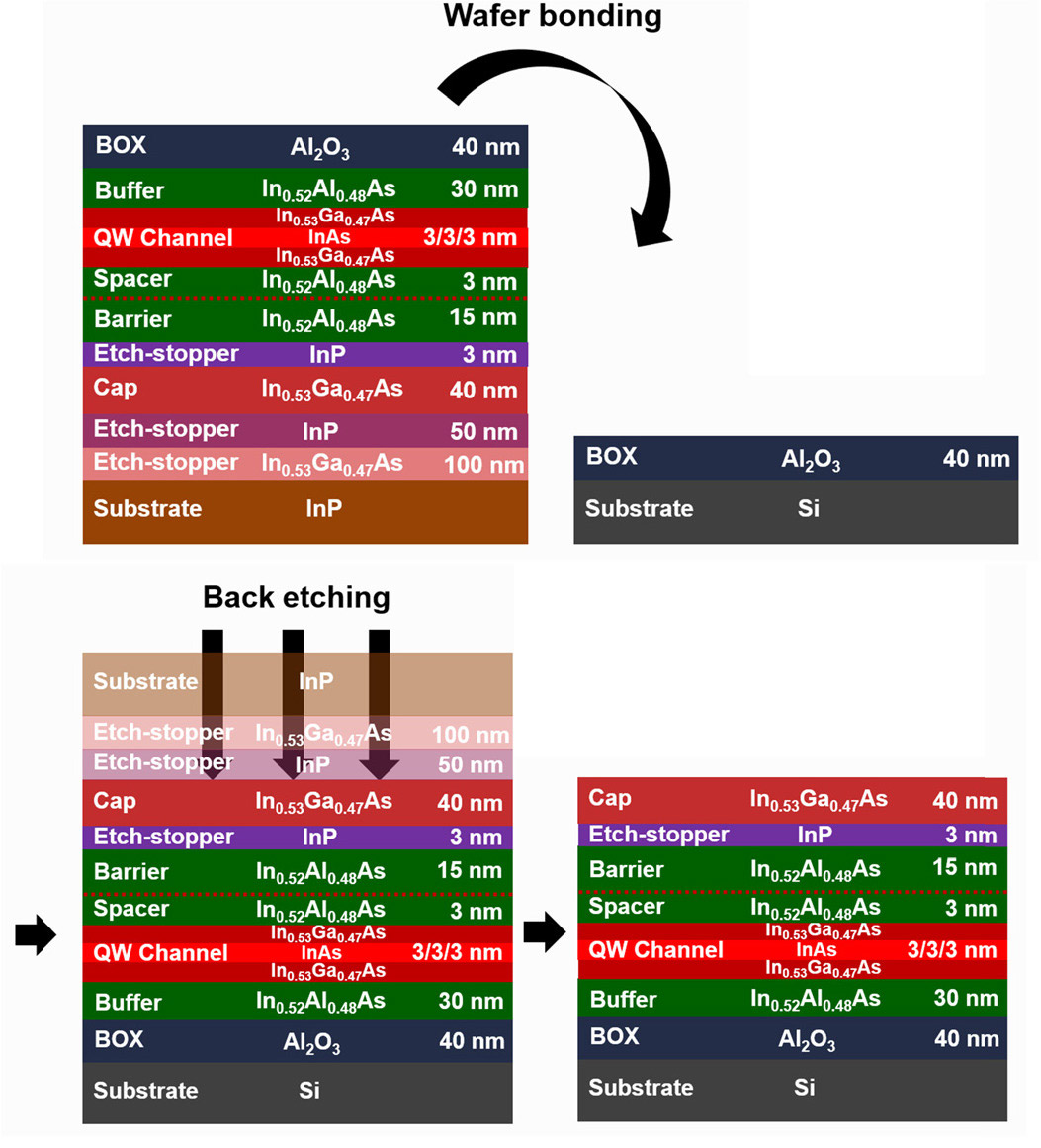
Figure 1: Fabrication process of InGaAs HEMT/Al2O3 BOX/Si structure.
The material was flipped and wafer-bonded to silicon, using 250°C atomic layer deposition (ALD) aluminium oxide (Al2O3) as the bonding layer and buried oxide (BOX). The bonding consisted of oxygen plasma activation and bonding at 200°C in vacuum. The InP growth substrate and etch stop layers were removed with various acidic mixtures, giving an InGaAs-on-insulator (InGaAs-OI) wafer.
Transistor fabrication (Figure 2) began with mesa etching with a phosphoric acid, hydrogen peroxide and water mixture. Ohmic contacts of non-alloyed molybdenum/gold were used for the source/drain. T-shaped gates with a LG of 125nm were formed through lithography, citric acid gate recess etch, and electron-beam evaporation of platinum/titanium/gold. The T-head was 400nm wide. The source-drain distance was 1.7μm. The process temperature was limited to less than 250°C.
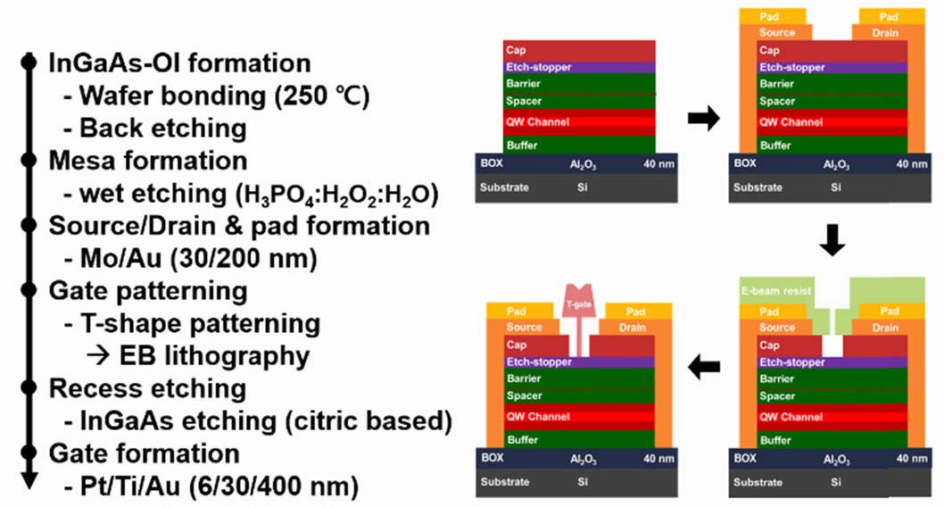
Figure 2: Process flow of InGaAs-OI HEMTs on silicon.
The subthreshold swing of the 125nm LG ‘short-channel’ device was 63.7mV/decade and 62.1mV/decade at drain biases of 0.05V and 0.5V, respectively. These values are close to the ~60mV/decade theoretical limit. The corresponding on/off current ratios were 105 and 106. The peak transconductance and maximum drain current were 0.5S/mm and 650mA/mm, respectively.
The gate leakage was less than 10nA/μm, due mainly to “the thick In0.52Al0.48As barrier (15nm) and spacer (3nm)”, according to the researchers. They add: “This low gate-leakage current is the essential figure-of-merit for developing analog applications such as low-noise amplifiers (LNAs) in terms of noise and power consumption.”
The source resistance was estimated at a relatively high 475.5Ω-μm. The researchers believe that around 78% of this can be traced to the thick barrier layer, which they hope to reduce in future work.
The frequency performance was characterized using measurements in the 1-40GHz range. The effect of parasitic elements was estimated using suitable test structures, and corrected to give ‘de-embedded’ results of 227GHz for the cut-off (fT) and 187GHz for the maximum oscillation (fMAX).
The researchers comment: “To the best of our knowledge, these values are the highest ever reported in the M3D RF transistors at given LG above 100nm.”
The relatively low fMAX was attributed to a large parasitic gate resistance. The team comments: “The fMAX of our InGaAs-OI HEMTs on Si can be further improved through tuning of the T-shape gate structure and optimized post-annealing process.”
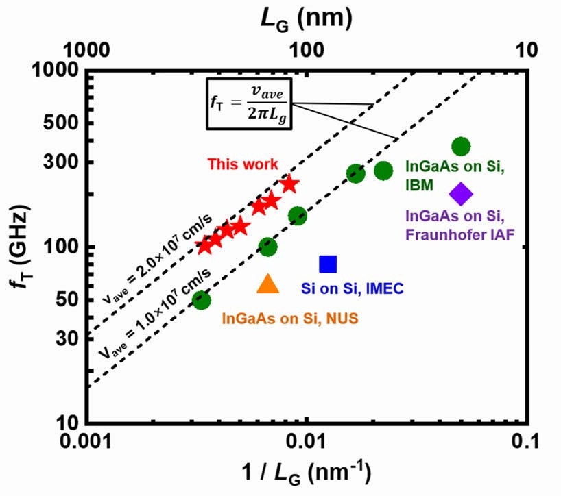
Figure 3: Benchmarks of III-V transistors on silicon, and silicon transistors on silicon, for M3D RF applications: fT versus 1/LG.
The researchers also looked at the performance of other groups reported in the scientific literature (Figure 3). The team expects to be able to improve on the present results through various techniques to boost RF performance.
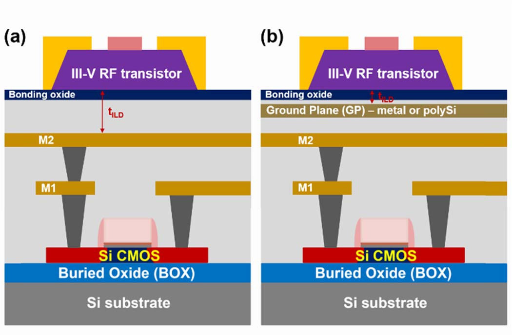
Figure 4: Schematic of simulated III-V transistor on silicon CMOS for M3D integrated RF applications (a) without ground plane and (b) with ground plane.
The team also performed simulations on III-V devices stacked over silicon circuitry (Figure 4). The researchers were particularly concerned about back-gate effects from bottom device electrodes and metal lines, particularly when a ground plane is used to reduce crosstalk between the top tier and bottom tier. These back-gate effects were found to severely impact RF performance, but were ameliorated by using thicker interlayer dielectric (ILD) layers, reducing parasitic capacitance.
InAs InGaAs InP substrates MBE InGaAs HEMT HEMT
https://doi.org/10.1109/TED.2021.3064527
The author Mike Cooke is a freelance technology journalist who has worked in the semiconductor and advanced technology sectors since 1997.


