


News: Microelectronics
18 February 2021
Hybrid III–V TFETs and MOSFETs on silicon
IBM Research Europe and École Polytechnique Fédérale de Lausanne (EPFL), both based in Switzerland, have developed a process for hybrid III-V tunnel field-effect transistors (TFETs) and metal-oxide-semiconductor field-effect transistors (MOSFETs) on a silicon platform [Clarissa Convertino et al, Nature Electronics, published online 8 February 2021, https://doi.org/10.1038/s41928-020-00531-3]. The use of band-to-band tunneling rather than thermionic emission enabled the TFETs to achieve much lower subthreshold swings (SSs) down to 42mV/decade, compared with 62mV/decade for the MOSFETs.
Low SS enables sharper digital switching or higher gain in amplifiers. The SS value represents the change in gate potential needed for a factor-of-ten increase in drain current in the subthreshold region.
The researchers explain the attraction of hybrid TFET/MOSFET circuitry: “III–V heterostructure TFETs are promising for low-power applications, but are outperformed by MOSFETs in terms of speed and energy efficiency when high performance is required at higher drive voltages.” They see particular opportunities for autonomous and wearable systems.
The team used a relatively conventional process for transistor formation as used in advanced silicon manufacturing for both the MOSFET and TFET. A lateral rather than vertical structure for the TFET offers the potential for device scaling. The team comments; “None of the existing III–V-based TFET demonstrations offer a clear path for integration with MOSFETs in a hybrid, scalable platform.”
The devices (Figure 1) featured indium gallium arsenide channels and source–drain regions of indium gallium arsenide (InGaAs) or gallium arsenide antimonide (GaAsSb). Doping for opposite majority carrier types in the source–drain materials enables a TFET p-i-n structure with the gate controlling the barrier width for band-to-band tunneling. In MOSFETs the gate controls the rate of thermionic emission.
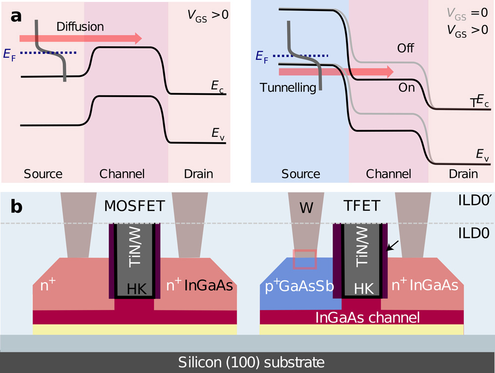
Figure 1: (a) Energy diagrams showing MOSFET (left) and TFET (right) valence and conduction bands and respective operating principles. (b) TFET and MOSFET cross sections, following last metallization.
The hybrid process featured replacement metal gate (RMG) and self-aligned raised source–drain (RSD) contact modules. The base material consisted of 10nm/20nm InGaAs/InP layers transferred to 4-inch silicon (100) using direct wafer bonding, resulting in a buried oxide (BOX) interface with the underlying silicon. The InGaAs was lattice-matched to the InP with 53% indium content.
The initial fabrication step consisted of dry etching the device isolation and fins that can be as thin as 20nm wide. A selective two-step dry/wet cyclic digital etch process was used to remove the base material from the source–drain region, allowing its epitaxial regrowth with doped material for the contacts in selective growth processes.
The ohmic source–drain contacts for the MOSFET consisted of n-InGaAs. By contrast, the TFET featured an n-InGaAs drain and p-GaAsSb source. Tin (Sn) was used for the n-inGaAs doping, while zinc (Zn) provided the p-GaAsSb. The lattice-matched GaAsSb consisted of 50% As and 50% Sb.
The gate stack consisted of high-k dielectric layers of aluminium oxide and hafnium dioxide, along with titanium nitride and tungsten (W) for the metal. The dielectric had a 1nm equivalent oxide thickness (EOT).
The devices were encapsulated in interlayer dielectric (ILD) with vias etched and filled with W for the contacts. The researchers comment: “The encapsulation represents a key feature of the developed process, because Sb-based compounds are particularly sensitive to oxidizing agents and suffer from poor etching selectivity. The source contact is partially exposed only at the end of the process and, as a result, it already appears purely crystalline 2nm from the contact interface.”
A TFET with 30nm gate length achieved a minimum SS of 49mV/decade with a 300mV drain bias (VDS). This was pushed down to 42mV/decade with VDS at 50mV. The MOSFET achieved a SS of ~62mV/decade, near the theoretical limit of 59.5mV/decade at room temperature (300K), for both drain bias conditions.
The current in the low bias condition fell off at high gate potential. The team suggests that this could be due either to a slight gate overlap or by a lower effective doping concentration in proximity of the tunnel junction. The researchers comment: “The effect is primarily visible at low VDS, where the reverse bias across the diode at the source–channel junction is smaller, thus it is probably not detrimental to device operation.”
The transistors also demonstrated high peak transconductance/drain current (gm/ID) ratios: 50/V for the TFET, and near the 39/V 300K limit for the MOSFET. Reducing the gate to 25nm only slightly increased the SS to 43mV/decade.
Cryogenic measurements found a decreasing SS for the TFET with lower temperature, reaching 10mV/decade at 4K. The cryogenic studies also found that trap-assisted tunneling was significant at lower temperatures, which indicates that removing these traps could further improve the SS performance.
The researchers claim that their TFETs demonstrate smaller SS values compared with “competing state-of-the-art TFET technologies” (Figure 2). The team adds: “In addition to the device performance, we also underline the uniqueness of this TFET platform in terms of scalability, compatibility with standard CMOS processes and co-integration with MOSFETs.”
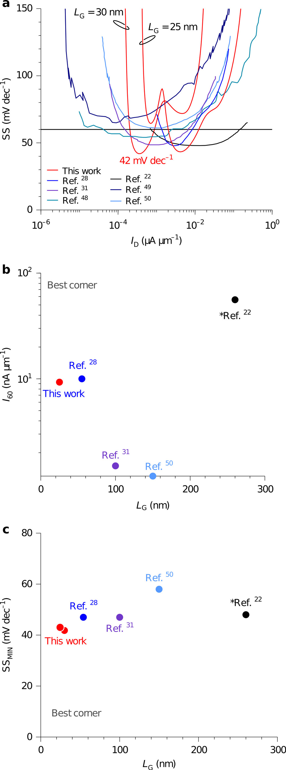
Figure 2: Benchmarking InGaAs/GaAsSb TFET performance: (a) SS versus ID, (b) I60 versus gate length (Lg), and (c) SS versus Lg.
None of the competing TFET processes considered by the team in their benchmark were CMOS-compatible. Further, only one of the competitors was produced in combination with a MOSFET. Only two of the reported TFETs were on silicon (111) or silicon-on-insulator (SOI) platforms. Four of the competitors presented used a vertical structure, with the remaining three lateral.
The device also features a short gate length and reasonable peak drain current in the region of SS less than 60mV/decade (I60).
Some funding for the work came from the European Commission’s 7th Framework (FP7) and Horizon 2020 programs.
https://doi.org/10.1038/s41928-020-00531-3
https://ec.europa.eu/research/fp7/index_en.cfm
https://ec.europa.eu/programmes/horizon2020/en
The author Mike Cooke is a freelance technology journalist who has worked in the semiconductor and advanced technology sectors since 1997.


