


News: Microelectronics
28 May 2020
Gallium nitride complementary logic on silicon using normally-off transistors
Researchers in the USA and China have integrated gallium nitride (GaN) n- and p-channel field-effect transistors (FETs) in complementary inverter circuits on silicon substrates [Nadim Chowdhury et al, IEEE Electron Device Letters, published online 13 April 2020]. The fabrication avoided complicated regrowth steps that could add to production costs. The circuit used enhancement-mode (normally-off) devices, reducing power consumption.
The researchers from Massachusetts Institute of Technology in the USA, Enkris Semiconductor Inc in China and Intel Corp in the USA see monolithic integration as a key way to increase switching speeds in power devices through reducing the parasitic inductance between driver circuitry and gate electrodes.
The team also claims “the first demonstration of operation at 300°C of any complementary logic technology, which confirm the potential of GaN for low-power digital applications under harsh-environment operation.” In addition, this could bring important applications for integrated CMOS driver circuits, CMOS logic, logic and signal conditioning under challenging conditions.
Enkris produced the epitaxial material on 6inch-diameter (111) silicon substrate through metal-organic chemical vapor deposition (MOCVD) – see Figure 1. The p-GaN layers were activated with an in-situ 750°C anneal in the reaction chamber. The threading dislocation density was in the range 109-1010/cm2, as determined by x-ray diffraction analysis.
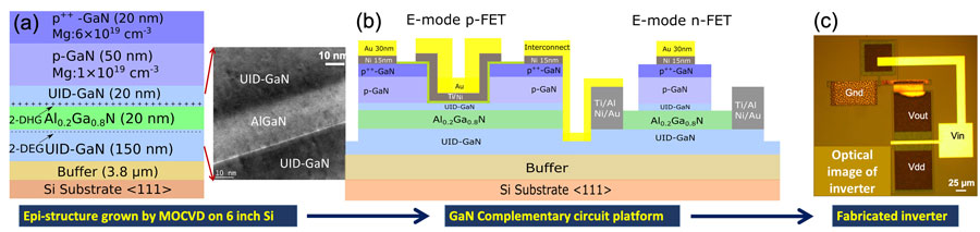
Figure 1: (a) Cross-sectional schematic of epitaxial structure and transmission electron micrograph image of channel regions; (b) Schematic of complementary circuit platform; (c) Optical image of fabricated logic inverter.
The epitaxial structure with aluminium gallium nitride (AlGaN) sandwiched between GaN layers was expected to result in two-dimensional electron (2DEG) and two-dimensional hole (2DHG) gases near the respective interfaces, due to charge polarization contrasts between the chemical bonds in the layers.
The n-FET region of the inverter was fabricated first with dry etch selectively removing the p-type layers, and forming annealed titanium/aluminium/nickel/gold (Ti/Al/Ni/Au) ohmic source/drain contacts with the 2DEG.
Dry mesa etching was then performed for electrical isolation of both the n- and p-FETs. Another dry etch created the gate recess for the p-FET. The sample was then dipped into heated tetramethylammonium hydroxide (TMAH) solution to remove the photoresist and smooth the surfaces resulting from the various dry etching steps.
Next, Ni/Au was applied to give the ohmic source/drain contacts of the p-FET and the gate electrode of the n-FET. The sample was then annealed in oxygen to oxidize the nickel to improve ohmic contact with the underlying p++-GaN layer.
The final steps formed the gate electrode of the p-FET and provided the interconnections for the inverter circuit: 20nm aluminium oxide atomic layer deposition (ALD) for the gate dielectric, and Ti/Au lift-off for the gate electrode and inverter interconnection. The widths of the n- and p-FETs were 12μm and 110μm, respectively.
As would be expected, the p-FET performed worse than the n-FET: the normalized on-resistances were 23kΩ-mm and 6Ω-mm, respectively, while the on/off current ratios were ~104 and ~107, in the same order. The threshold of the n-FET was +0.2V, and the p-FET -1V. Both devices are described as having “good pinch-off behavior”.
The researchers comment: “The poor performance of p-FET in terms of ON-resistance can mainly be attributed to the higher ohmic contact resistances”.
With a 5V supply voltage (VDD), the inverter circuit is reported to have a “very good switching transition from high to low voltage with a swing voltage Vswing of 4.91V” (Figure 2). An input voltage 0.59V yielded a maximum voltage gain of ~27V/V. The 27V/V figure is claimed to be a record by the researchers.
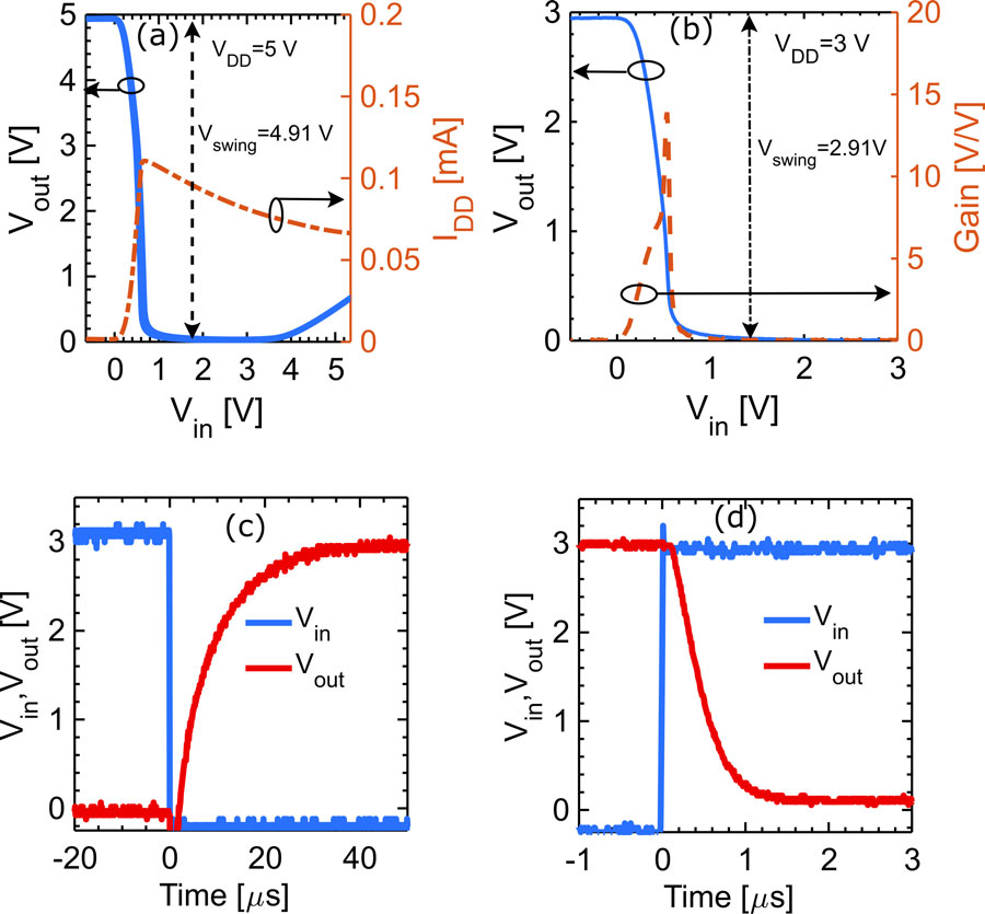
Figure 2: Direct current transfer curve of fabricated inverter with (a) 5V and (b) 3V supply. Transient response showing (c) rise and (d) fall times.
The high-low transition occurs around 0.2V due to the low threshold of the n-FET – an ideal transition would occur around 2.5V, half the value of VDD. The researchers suggest that the n-FET threshold could be increased with a fin-FET trigate structure.
At 5V VDD, there is a rise in response at higher voltages above 3.6V, due to “gate leakage from the p-GaN gated n-FET”, according to the team. Restricting the VDD to 3V eliminated the gate leakage problem. Under these conditions the swing was 2.91V and the maximum gain was ~15V/V.
Keeping the VDD at 3V, the researchers subjected the circuit to pulsed signals between -0.2V and 3V with a 100ns ramp. The fall time at the output was 1μs, while the rise time was 20μs. The researchers suggest that these values represent upper limits since the oscilloscope used had a relatively high input capacitance of 350pF.
Increasing the operating temperature of the device up to 300°C was found to reduce the gain, along with the maximum available voltage swing. The reduced swing is attributed to a lowering of the on/off current ratio of the p-FET at high temperature. The higher temperature also had adverse impacts on high- and low-level noise margins: 2.24V/0.12V and 1.75V/0.04V at room temperature and 300°C, respectively.
GaN AlGaN FETs CMOS MOCVD Silicon substrates
https://doi.org/10.1109/LED.2020.2987003
The author Mike Cooke is a freelance technology journalist who has worked in the semiconductor and advanced technology sectors since 1997.


