


News: Optoelectronics
22 May 2020
Lower thresholds for indium arsenide quantum dash lasers on silicon
Hong Kong University of Science and Technology has reduced the threshold current for indium arsenide (InAs) quantum dash (QDash) laser diodes on an indium phosphide (InP) on on-axis (001) silicon (Si) template [Wei Luo et al, Appl. Phys. Lett., vol116, p142106, 2020].
The devices emitted at 1.3μm wavelength, but the researchers believe that tuning the metal-organic chemical vapor deposition (MOCVD) growth process could enable ~1.5μm emissions as well. These wavelengths fall in the key optical communication O- and C-bands of 1260-1360nm and 1530-1565nm.
The team comments: “This platform offers a feasible path toward achieving O-band and C-band lasers using the same InP-based material system by the manufacturing-friendly MOCVD process, benefiting silicon-based on-chip optical interconnects.”
Confined QDash regions enable lower threshold, less temperature sensitivity, and larger modulation bandwidths, compared with quantum well light-emitting structures. Further, the confinement of QDashes results in them being less subject to defects such as threading dislocations.
The use of on-axis (001) Si opens the way to integration with efficient complementary metal-oxide-semiconductor (CMOS) mainstream electronics, lower material costs, and economies of scale from larger-diameter substrates.
The researchers used low-pressure MOCVD to build the epitaxial material on gallium arsenide (GaAs) on V-grooved (GoVS) and unpatterned (GoPS) on silicon.
One defect reduction technique involved 5x thermal cyclic annealing (TCA) at 800°C after a high-temperature 600°C step of GaAs growth on GoVS. The GoPS template used a 4-cycle TCA. Further measures included two superlattice layers of InGaAs/GaAs in the GaAs buffer. The total thickness of the GaAs part of the template structure on GoVS was 2μm, while the GoPS structure was only 1.1μm.
The 3.1μm InP template section also included superlattices to deflect and filter out threading dislocations. The researchers estimated that the defect density of InP/GoVS and InP/GoPS templates were 2.75x10⁸/cm2 and 3.54x10⁸/cm2, respectively, according to transmission electron microscope analysis. The researchers point out that recent advances in GaAs on Si templates have resulted in defect densities of order 106/cm2.
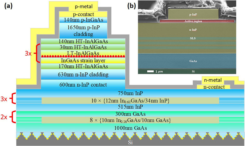
Figure 1: (a) Schematic of InAs/InAlGaAs QDash laser device on V-grooved Si; (b) color-enhanced scanning electron microscope image of Fabry–Pérot laser device with mirror-like facet.
Growth continued to the laser layers with n-InP, InAs/InAlGaAs QDashes, and p-InGaAs/InP. Zinc was used as the p-dopant. The QDashes were self-assembled with a 5-second growth interruption, allowing the 510°C InAs to separate into dashes. The indium gallium aluminium gallium arsenide (InAlGaAs) matrix for the dashes was grown in two steps: first at low temperature to avoid desorbtion of the dashes, and then at 630°C as a spacer from the next QDash layer.
The density of QDashes was estimated to be 2.5x10¹⁰/cm2, according to atomic force microscopy. The accumulated strain in the structure resulted in some vertical alignment between the dashes in the different layers.
Photoluminescence measurements showed a 45nm difference in emission wavelengths for the GoVS and GoPS templates: ~1300nm for GoPS and ~1350nm for GoVS. “The wavelength discrepancy is speculated to be related to the different residual strain and surface temperature of the two templates,” the team writes.
The photoluminescence on the GoVS template was about half the intensity of that of the GoPS structure. Even so, the laser diodes on GoVS had a lower threshold, compared with the GoPS sample (Figure 2).
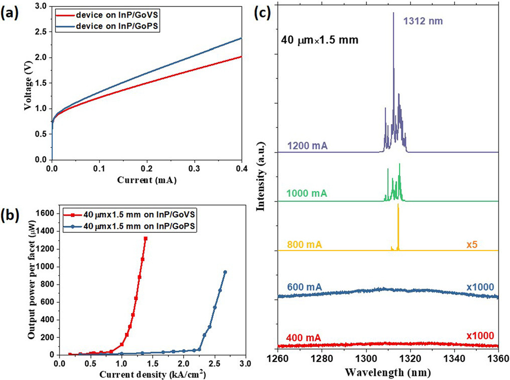
Figure 2: (a) Current–voltage curves of different size InAs QDash lasers grown on InP/GoVS and InP/GoPS; (b) current light output power curves of 40μmx1.5mm InAs QDash lasers on InP/GoVS and InP/GoPS; (c) emission spectrum of 40μmx1.5mm InAs QDash lasers.
The researchers explain: “This is primarily because the QDash growth condition was initially optimized on InP/GoPS instead of on InP/GoVS, resulting in a weaker PL intensity for QDashes on InP/GoVS. However, the material quality, regarding defect density and surface roughness, of the InP/GoVS accounts for the more appealing device result.”
The team, therefore, expects that further optimization will improve the photoluminescence on GoVS and enable continuous-wave operation. The present devices were only tested under 400ns, 0.5% duty cycle pulsed operation at room temperature.
The lowest threshold current density for the laser diodes on GoVS came in at 1.05kA/cm2 for a 40μmx1.5mm cavity. The single-facet light output power reached 22mW without roll-over in a 20μmx1mm device.
A 40μmx1.5mm laser cavity on GoPS managed a 2.24kA/cm2 threshold current density. A 20μmx1mm device on GoPS continued lasing up to 70°C. Devices on GoVS are said to have a “similar” temperature performance.
As the current increased above threshold, multi-mode spectra were produced in these devices. The emissions were around 1.3μm wavelength. The researchers say that tuning the QDash growth could produce 1.5μm emission.
The active QDash region was sandwiched in a separate-confinement heterostructure with InAlGaAs spacers and InP cladding.
The materials were processed into ridge-waveguide lasers through photolithography, dry etching, and metallization. The metal contacts were placed laterally on the top-side of the epitaxial layers. This avoided current flow through the highly defective buffer layers.
On InP substrate, vertical top-to-bottom current flow is possible, which has advantages in terms of avoiding current crowding and so on. The device wafers were finally thinned to about 100μm thick, and cleaved into wafer bars. The cleaved mirror facets were not coated to enhance reflectivity.
InAs quantum dot lasers InP InAlGaAs MOCVD CMOS
https://doi.org/10.1063/1.5145031
The author Mike Cooke is a freelance technology journalist who has worked in the semiconductor and advanced technology sectors since 1997.


