


News: Microelectronics
5 March 2020
Barium titanate and aluminium gallium nitride power electronics
Ohio State University and University of South Carolina in the USA have been exploring the use of the extreme-permittivity dielectric barium titanate (BaTiO3) perovskite oxide to increase breakdown voltage and to reduce resistance in aluminium gallium nitride (AlGaN) electronics [Towhidur Razzak et al, Appl. Phys. Lett., vol116, p023507, 2020].
AlGaN is of interest in power electronics as a wide-bandgap semiconductor with a high critical breakdown electric field value of more than 9MV/cm (when the aluminium content exceeds 50%), good low-field electron transport characteristics, and high saturation velocity. Such features could enable high-power, high-frequency radio signal generation, along with allowing the handling of high power densities in electronic circuitry.
However, realizing these potential benefits in actual performance requires meeting a number of challenges for device structures with non-uniform field distributions. The researchers see BaTiO3 as having benefits for device scaling, enabling AlGaN-based transistors to access radio frequency (RF) performance.
The team explains: “Extreme-permittivity dielectrics enable improved breakdown due to two reasons. First, a high-dielectric-constant layer greatly reduces the peaking or non-uniformity in the lateral electric field between the gate to drain for lateral transistors or anode to cathode for lateral diodes and results in a higher breakdown voltage and higher average breakdown field due to a more uniform electric field distribution.”
The researchers also point to potential high-breakdown benefits from BaTiO3 use in gallium oxide (Ga2O3) structures. Due to the wider bandgap of these materials being associated with lower electron mobility compared with GaN, the team suggests that scaling would compensate for high sheet resistance. Further, the use of high-k dielectrics in transistor gate stacks enables better electrostatic control of carrier flow in channels with lower output conductance and higher transconductance.
A potential drawback of high-k materials is extension of the drain depletion region and an increase the gate-to-channel capacitance. Such factors would tend to reduce cut-off frequencies. The researchers comment: “It is therefore important to properly optimize the thickness of the high-permittivity region to manage the trade-off between field management and gate–drain capacitance.”
The researchers used 3μm-thick AlN on sapphire templates to grow AlGaN by low-pressure metal-organic chemical vapor deposition (LP-MOCVD). The template layer was grown by the same technique at 1250°C. Further layers consisted of 500nm undoped intrinsic i-Al0.58Ga0.42N at ~1100°C, folllowed by 60nm heavily silicon-doped n-Al0.58Ga0.42N.
Selective molecular beam epitaxy (MBE) was used to construct the ohmic cathode contact (Figure 1). The patterned hard mask for the MBE was silicon dioxide. The material in the pit consisted of 50nm heavily doped n-Al0.58Ga0.42N and 50nm reverse Al-composition graded AlGaN, also heavily doped.
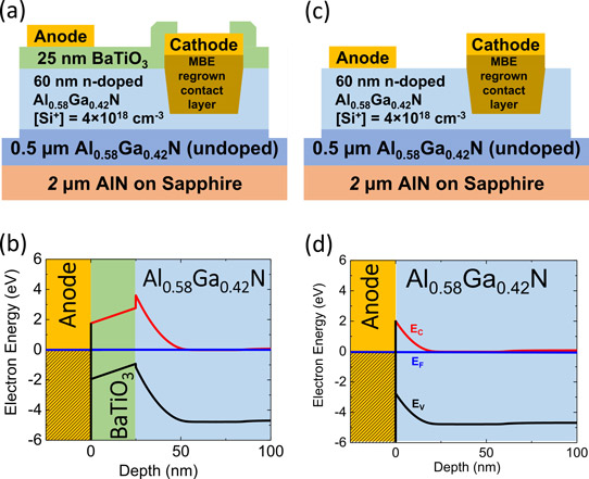
Figure 1: (a) Schematic of lateral Pt/BaTiO 3/Al0.58Ga0.42N heterojunction diode, (b) modeled band-diagram under anode, (c) schematic of fabricated lateral Pt/Al0.58Ga0.42N control Schottky diode, and (d) modeled band-diagram.
“The purpose of the reverse-Al-composition graded n++ AlGaN layer is to minimize abrupt conduction band offsets and facilitate low-resistance non-alloyed Ohmic contact formation,” the team explains.
The silicon dioxide hard mask was removed with a wet buffered oxide etch. The Ohmic contact metal stack was titanium/aluminium/nickel/gold. Device isolation was achieved with mesa etching through an inductively coupled plasma reaction-ion etch (ICP-RIE) process.
The high-permittivity BaTiO3 film was deposited using RF sputtering, giving a dielectric constant of about 60. The film was expected to be nanocrystalline/amorphous. Control Schottky diode samples without the BaTiO3 were created by etching the material away with a sulfur hexafluoride ICP-RIE process. The anode consisted of platinum/gold.
The control Schottky diode had a 0.9V turn-on voltage, compared with 1.5V for the heterojunction diode with BaTiO3. These values are significantly lower than is typical in AlGaN p-n or p-i-n diodes. “This suggests that the BaTiO3/AlGaN interface presents relatively small barriers to electron transport, in contrast to conventional metal-oxide-semiconductor junctions where a large voltage would be needed to achieve turn-on of the current,” the researchers comment.
The differential on-resistance was 31mΩ-cm2 for the control and 56mΩ-cm2 for the BaTiO3/AlGaN heterojunction device. The corresponding breakdown voltages were 42V and 155V for anode-cathode gaps of 0.19μm and 0.18μm, respectively, as determined by scanning electron microscope (SEM) inspection. The higher breakdown in the heterojunction device is attributed to “a reduced peak field and the suppression of anode leakage current”.
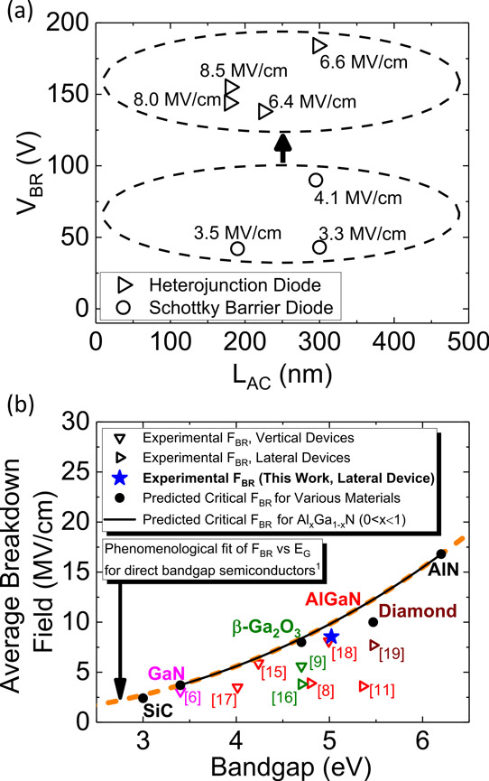
Figure 2: (a) Breakdown performance for lateral Pt/BaTiO3/Al0.58Ga0.42N heterojunction and AlGaN Schottky barrier diodes with anode–cathode distance (LAC) less than 500nm. (b) Reported experimental average breakdown fields in semiconductor devices achieved to date (pink: GaN, green: Ga2O3, red: AlGaN, and brown: diamond). Dashed orange line phenomenological fit of critical breakdown field (FBR) versus direct bandgap (EG). Solid black circles predicted critical breakdown fields.
Calculations suggest that the peak vertical field was 3.15MV/cm and the lateral field was 1.58MV/cm in the Schottky device, resulting in a total average field of 3.5MV/cm. The heterojunction had the same vertical field, but increased the lateral value to 7.94MV/cm. The average total breakdown electric field is estimated to be 8.5MV/cm.
The team comments: “The value reported in this work, 8.5MV/cm, is the highest reported experimental average breakdown field for any semiconductor material.”
The researchers hoped for even higher breakdown voltages, based on the theoretical maximum breakdown field of 9.7MV/cm with “optimization of the BaTiO3 thickness and growth conditions together with the exploration of potential integration of field plate structures”.
Barium titanate AlGaN LP-MOCVD MBE
https://doi.org/10.1063/1.5130590
The author Mike Cooke is a freelance technology journalist who has worked in the semiconductor and advanced technology sectors since 1997.


