


News: Microelectronics
18 March 2020
Room-temperature bonded GaN/diamond interface improves cooling of HEMTs
A room-temperature bonding technique for integrating wide-bandgap materials such as gallium nitride (GaN) with thermally conducting materials such as diamond could boost the cooling effect on GaN devices and facilitate better performance through higher power levels, longer device lifetime, improved reliability and reduced manufacturing costs, reports the USA’s Georgia Tech, in collaboration with Japan’s Meisei University and Waseda University (Zhe Cheng et al, ‘Interfacial Thermal Conductance across Room-Temperature-Bonded GaN/Diamond Interfaces for GaN-on-Diamond Devices’, ACS Appl. Mater. Interfaces, 2020, 12, 8376−8384). The work was supported by a multi-disciplinary university research initiative (MURI) project (grant no. N00014-18-1-2429) from the US Office of Naval Research (ONR). The technique could have applications for wireless transmitters, radars, satellite equipment and other high-power and high-frequency electronic devices.
The surface-activated bonding technique uses an ion source in a high-vacuum environment to first clean the surfaces of the GaN and diamond, which activates the surfaces by creating dangling bonds. Introducing small amounts of silicon into the ion beams facilitates forming strong atomic bonds at room temperature, allowing the direct bonding of the GaN and single-crystal diamond that allows the fabrication of high-electron-mobility transistors (HEMTs).
The resulting interface layer from GaN to single-crystal diamond is just 4nm thick, allowing heat dissipation up to two times more efficient than in state-of-the-art GaN-on-diamond HEMTs by eliminating the low-quality diamond left over from nanocrystalline diamond growth. Diamond is currently integrated with GaN using crystalline growth techniques that produce a thicker interface layer and low-quality nanocrystalline diamond near the interface. Additionally, the new process can be performed at room temperature using surface-activated bonding techniques, reducing the thermal stress applied to the devices.
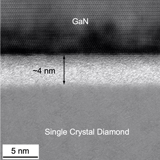
Picture: Cross-section bright-field high-resolution STEM images of GaN-diamond interfaces bonded by surface-activated bonding technique. (Zhe Cheng, Georgia Tech)
“This technique allows us to place high-thermal-conductivity materials much closer to the active device regions in gallium nitride,” notes Samuel Graham, the Eugene C. Gwaltney Jr School Chair and Professor in Georgia Tech’s George W. Woodruff School of Mechanical Engineering. “The performance allows us to maximize the performance for gallium nitride on diamond systems. This will allow engineers to custom design future semiconductors for better multi-functional operation.”
For high-power electronic applications using materials such as GaN in miniaturized devices, heat dissipation can be a limiting factor in power densities imposed on the devices. By adding a layer of diamond, which conducts heat five times better than copper, engineers have tried to spread and dissipate the thermal energy.
However, when diamond films are grown on GaN, they must be seeded with nanocrystalline particles about 30nm in diameter, and this layer of nanocrystalline diamond has low thermal conductivity – which adds resistance to the flow of heat into the bulk diamond film. In addition, the growth takes place at high temperatures, which can create stress-producing cracks in the resulting transistors.
“In the currently used growth technique, you don’t really reach the high-thermal-conductivity properties of the microcrystalline diamond layer until you are a few microns away from the interface,” Graham says. “The materials near the interface just don’t have good thermal properties. This bonding technique allows us to start with ultra-high thermal conductivity diamond right at the interface.”
By creating a thinner interface, the surface-activated bonding technique moves the thermal dissipation closer to the GaN heat source.
“Our bonding technique brings high-thermal-conductivity single-crystal diamond closer to the hotspots in the GaN devices, which has the potential to reshape the way these devices are cooled,” believes the paper’s first author Zhe Cheng, a recent Georgia Tech Ph.D. graduate. “And because the bonding takes place near room temperature, we can avoid thermal stresses that can damage the devices.”
That reduction in thermal stress can be significant, going from as much as 900MPa to less than 100MPa with the room-temperature technique. “This low-stress bonding allows for thick layers of diamond to be integrated with the GaN and provides a method for diamond integration with other semiconductor materials,” Graham says.
Beyond GaN and diamond, the technique can be used with other semiconductors, such as gallium oxide, and other thermal conductors such as silicon carbide. Graham says that the technique has broad applications to bond electronic materials where thin interfacial layers are advantageous.
“This new pathway gives us the ability to mix and match materials,” he says. “This can provide us with great electrical properties, but the clear advantage is a vastly superior thermal interface. We believe this will prove to be the best technology available so far for integrating wide-bandgap materials with thermally conducting substrates.”
In future work, the researchers plan to study other ion sources and evaluate other materials that could be integrated using the technique.
“We have the ability to choose processing conditions as well as the substrate and semiconductor material to engineer heterogenous substrates for wide-bandgap devices,” Graham says. “That allows us to choose the materials and integrate them to maximize electrical, thermal and mechanical properties.”
Diamond thermal management GaN HEMT


