


News: Microelectronics
7 July 2020
II-VI relying on GE’s IP to conquer power SiC markets
As announced at the end of June, engineered materials and optoelectronic component maker II-VI Inc of Saxonburg, PA, USA – which manufactures silicon carbide (SiC) substrates – has licensed SiC technology from General Electric with a view to moving into power device and module manufacturing. Just like II-VI’s main competitors in the SiC wafer market – US-based Cree/Wolfspeed and Japan-based Rohm Group Company (including SiCrystal) – the new licensee aims to capitalize on the growing market demand for SiC-based power electronics, driven by the fast development of electric vehicle and hybrid electric vehicle (EV/HEV) applications.
General Electric’s SiC power device technology has been reviewed by Knowmade in its report ‘Power SiC Patent Landscape 2019 (MOSFETs -SBDs – Modules)’. “GE’s patenting activity took off in the late 2000s, focusing on the planar device architecture of SiC MOSFETs,” notes Rémi Comyn PhD, technology & patent analyst Compound Semiconductors and Electronics at Knowmade. Indeed, as of 2020, GE’s patent portfolio includes over 30 patent families (i.e. single inventions patented in multiple countries) related to SiC MOSFETs, grouping over 30 granted patents and 40 pending patent applications, which reflects GE’s global IP strategy, extending over USA, China, Japan and Europe.
According to Knowmade’s analysis, General Electric was the most active IP player on planar SiC MOSFET technology, but still a challenger for Cree/Wolfspeed and Mitsubishi Electric (as illustrated in Figure 1). Starting its patenting activity in the 1990s, Cree took the leadership on planar SiC MOSFETs and currently holds over 90 granted patents worldwide, including numerous key patents in the domain, while GE’s patent portfolio was mainly composed of pending patent applications as of 2018. Yet, within the last couple of years, GE has managed to convert a promising IP potential into a strong patent portfolio with more and more enforceable patents (Figure 1).
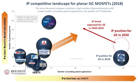
Figure 1: Evolution of GE’s IP leadership in the planar SiC MOSFET patent landscape.
Furthermore, GE’s current patenting activity related to SiC MOSFET technology has now shifted towards power converters based on this technology. “We’re observing a slowdown in GE’s patenting activity in the SiC MOSFET patent landscape, with only a couple of new inventions published since 2018, indicating that GE’s SiC MOSFET technology has reached a high level of maturity,” says Comyn. “GE’s patenting activity is now mainly related to the extension of US priority patents worldwide.” Apart from SiC MOSFETs and SiC-based converters, GE also published several new inventions related to low-inductance SiC power modules, e.g. patent US 10,021,802 (2018) and patent US 9,893,646 (2017).
Interestingly, numerous patents filed by GE focus on issues related to the gate structure of planar SiC MOSFET, e.g. the mitigation of negative-bias temperature instability in the threshold voltage of SiC MOSFET devices. In patent US 10,367,089, GE’s inventors insert a dielectric layer deposited on the gate electrode and a remedial layer deposited on, within or below the dielectric layer in order to limit the variation in threshold voltage below 1V (Figure 2).
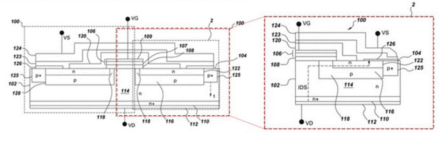
Figure 2: (Patent US 10,367,089) the remedial layer 123 deposited on the dielectric layer 120 and configured to mitigate negative-bias temperature instability.
Moreover, GE’s patent portfolio addresses different building blocks of planar SiC technology, such as:
- systems and methods for ohmic contacts (based on an annealed nickel silicide layer) in SiC devices (patent US 9,230,807);
- electric field shielding in SiC MOSFET devices having an optimization layer (patent US 10,096,681);
- a planar SiC MOSFET device with reduced electric field at the sharp corners of a gate electrode (Figure 3), for enhanced device reliability (patent application EP 3,108,507); and
- a non-planar SiC n-channel DMOSFET device with increased channel periphery (patent US 9,024,328).
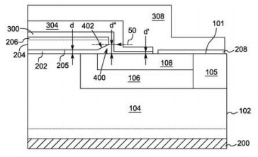
Figure 3: (Patent application EP 3,108,507) The gate insulating layer (202), e.g. SiO2, has greater thickness at the corner of the layer than at the center. The gate electrode (204) comprises a polycrystalline silicon layer.
More recently, GE has disclosed an invention related to gate networks having positive temperature coefficients of resistance (PTC) for SiC power devices (2019) and a second invention focusing on SiC devices having improved electric field suppression over the termination regions (2020).
In 2013, GE qualified its technology for the automotive industry (AEC-Q101, 200°C). In late 2016, the company entered high-volume production of SiC power devices at the New York Power Electronics Manufacturing Consortium (NY-PEMC) facility (SUNY Poly’s 150mm SiC fab in Albany, NY, USA), in addition to low-volume production at its existing 4-inch pilot SiC fab (GE Global Research Center in Niskayuna, NY, USA). In 2017, in the framework of NY-PEMC, GE announced a manufacturing partnership with Danfoss to produce SiC power modules in Utica (NY, USA). Interestingly, Danfoss is a new entrant in the ‘Power SiC Patent Landscape 2019’ report and filed four pending applications in 2018 related to the optimization of high-power-conversion-efficiency and high-power-density modules based on SiC power devices.
The patent agreement between II-VI and General Electric will further promote the adoption of planar SiC MOSFET technology for the electrification of systems including, for example, industrial infrastructure, large data centers and vehicles (EV/HEV). “While most automotive-focused patent applicants such as Toyota Motor and Rohm seem to place the emphasis on trench SiC MOSFET technology for automotive applications, we’re also observing partnerships involving planar SiC MOSFET suppliers such as Cree/Wolfspeed to develop SiC-based automotive applications,” comments Comyn. By way of example, in November 2019, a strategic partnership was established between Cree/Wolfspeed and automotive supplier ZF to enhance the electric powertrain with SiC-based inverters.
II-VI licenses GE’s SiC power electronics technology
II-VI signs multi-year agreement of over $100m to supply SiC substrates
New York Power Electronics Manufacturing Consortium produces its first SiC-based patterned wafers
GE and SUNY Poly developing SiC power electronics packaging facility at QUAD C
GE to lead $500m five-year State-funded New York Power Electronics Manufacturing Consortium


