


News: LEDs
17 December 2020
Boosting blue light emission with silica array substrates
Wuhan University in China has reported a 16.5% improvement in light output power for indium gallium nitride (InGaN) blue light-emitting diodes (LEDs) grown on patterned sapphire with silica array (PSSA) substrates, compared with a similar device grown on patterned sapphire [Shuyu Lan et al, Optics Express, vol. 28, p38444, 2020]. The team comments: “This work demonstrates a significant step forward in the development of high-performance LEDs for high-resolution display.” Other potential applications could come from visible light communications (VLC), automotive front lighting, and general lighting.
The researchers credit the improvements to better crystal quality and enhanced light extraction through the sapphire substrate in the flip-chip devices.
The PSSA was prepared using photoresist thermal-reflow and plasma etch (www.semiconductor-today.com/news_items/2020/jan/wuhan-300120.shtml) to create 2.8μm-diameter silica/silicon dioxide (SiO2) cones with 3.0μm center-to-center spacing. The cone height was 2μm. Further plasma etch was performed after the cone formation, cutting into the sapphire, giving thin pedestals for the cones.
These sapphire pedestals are found to bend the threading dislocations (TDs) away from the active regions of the structure. The use of SiO2 reduces coalescence boundaries in GaN, which leads to less misfit strain, further reducing TD density.
The team adds: “Since no GaN islands formed on the silica array cone sidewall regions, the LED grown on PSSA effectively decreased the misfit existing in the coalescence boundary of GaN grown on the sidewall regions and c-plane region of the substrate.”
III-N growth began with aluminium sputtering at 650°C in a nitrogen, oxygen and argon gas mix, creating a 15nm aluminium nitride (AlN) nucleation layer. The rest of the LED structure (Figure 1) was grown using metal-organic chemical vapor deposition (MOCVD): 3μm GaN buffer, 2.5μm n-GaN contact, 260nm lightly doped n-GaN, 3x 1.5nm/30nm In0.02Ga0.98N/GaN interlayer (IL), 6x 1.5nm/9nm In0.05Ga0.95N superlattice (SL), 9x 3nm/12nm In0.16Ga0.84N/GaN multiple quantum well (MQW) active region, 15nm p-GaN, 25nm p-Al0.2Ga0.8N electron-blocking layer, and 80nm p-GaN contact.
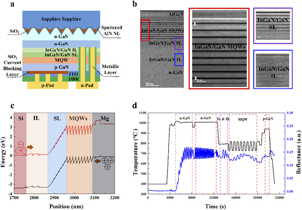
Figure 1: (a) Schematic GaN-based flip-chip LED structure on PSSA. (b) Cross-sectional scanning transmission electron micrograph. (c) Simulated energy-band diagram. (d) In-situ reflectance and temperature transients during epitaxial growth.
The researchers explain: “The use of In0.02Ga0.98N/GaN IL and In0.05Ga0.95N SL reduced the effective barrier heights for both electrons in the conduction band and holes in the valence band, leading to an increased effective electron capture rate.”
X-ray analysis gave a TD density of 1.3x10⁸/cm2, compared with 3.3x10⁸/cm2 for a similar structure grown on patterned sapphire substrate (PSS).
The structure was flipped in the processed 380μmx760μm LED, with the light emerging mainly from the sapphire side. The emission wavelength under 60mA current injection was 445nm (blue). By contrast, a PSS device had a longer wavelength of 452nm. The longer wavelength was attributed to the effect of piezoelectic fields arising from extra strain in the PSS-based structure. These fields shift the performance due to the quantum-confined Stark effect (QCSE).
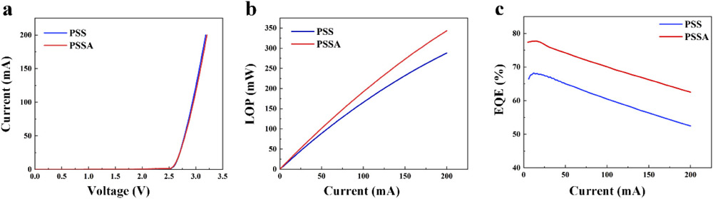
Figure 2: (a) Current-voltage and (b) current-LOP characteristics of LEDs grown on PSS and PSSA. (c) EQEs versus current.
The PSSA substrate also gave benefits in terms of light output power (LOP) and external quantum efficiency (EQE): 225.7mW at 120mA and 77.7% (peak), respectively, compared with 193.8mW and 67.8% for PSS. The improved performance is attributed to both enhanced crystal quality and superior light extraction efficiency.
Light extraction benefited from the presence of SiO2 with a 1.45 refractive index closer to that of air, 1, compared with sapphire (1.78) or GaN (2.46). The lower refractive index of SiO2 reduces the amount of total internal reflection, transmitting light to the outside world more readily.
Sapphire silicon dioxide cone array growth substrate InGaN LEDs
https://doi.org/10.1364/OE.413088
The author Mike Cooke is a freelance technology journalist who has worked in the semiconductor and advanced technology sectors since 1997.


