


News: Microelectronics
10 December 2020
Vertical power trigate SiC MOSFET
Purdue University and Sonrisa Research Inc in the USA report “a dramatic reduction in specific channel resistance” for a novel vertical power tri-gate metal-oxide-semiconductor field-effect transistor (MOSFET) in 4H-polytype silicon carbide (SiC) that incorporates sub-micron FinFET channels [Rahul P. Ramamurthy et al, IEEE Electron Device Letters, published online 24 November 2020].
Combined with wafer thinning, the structure could enable more than a 2x reduction in on-resistance, “permitting twice as many devices on a wafer and dramatically reducing the cost of SiC power MOSFETs in the 650V regime,” according to the team.
The fin structures increase the effective width of the current-carrying regions without increasing the device area. Reducing on-resistance is particularly important in SiC devices using inversion layer channels, since the mobility is reduced by a factor of 10 relative to silicon. The compensating factor for interest in SiC devices is its higher blocking capabilities, giving higher breakdown voltages as a result of higher critical electric fields, which is a property it shares with the fellow wide-bandgap material gallium nitride (GaN).
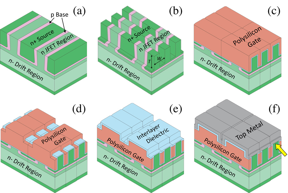
Figure 1: Outline of tri-gate MOSFET fabrication sequence: (a) implant p-base and n+ source regions, (b) etch trenches, (c) deposit gate oxide and polysilicon gates, (d) pattern polysilicon gates, (e) form ILD, and (f) clear thin oxide on fins with BHF dip, form ohmic contacts and deposit top metal.
The researchers, two of whom have since moved on to Intel Corp and Wolfspeed Inc respectively, particularly targeted 650V applications, since some two-thirds of power applications fall within ratings less than 1000V.
The epitaxial wafer used consisted of a 350μm-thick heavily doped n+ 4H-SiC substrate, a 5.2μm 1.4x10¹⁶/cm3 n-type drift layer, and a 1.6μm 1.0x10¹⁷/cm3 n-type junction FET layer. Double ion implantation with MeV-level acceleration resulted in the formation of 2μm-deep 5μm-wide retrograde p-type base regions, in which 1.3μm-deep 4μm-wide n+ source regions were added using a self-aligned short-channel technique. The p-type base regions were formed in stripes separated by 4.5μm.
The channel was formed by etching fins across the implanted stripes: 0.8μm deep, 0.5μm wide and spaced by 0.5μm. The etched surfaces were smoothed with hydrogen plasma etch at 1500°C and 15kPa pressure.
The gate stack consisted of low-pressure chemical vapor deposition (LPCVD) polysilicon, thermally oxidized at 580°C to create a 47nm insulator layer, and diffusion-doped polysilicon forming the gate electrode. The oxidized polysilicon insulator was thermally annealed at 1175°C in nitric oxide (NO) before the electrode deposition. The gate electrodes were patterned into 7.5μm-wide stripes to allow access in the 2μm-wide gaps to the source regions.
Further thermally oxidized polysilicon was deposited as a thick interlayer dielectric (ILD). The top of the fins in the source region were cleared of insulating material with a buffered hydrofluoric (BHF) acid dip before self-aligned nickel contacts were deposited and annealed. The device was completed with top metal layers of titanium and gold.
The resulting device was aimed at 650V blocking, enabled by floating-field-ring edge terminations. Avalanche breakdown occurred at 706V, and the gate-oxide broke under ~9MV/cm electric field.
The gate threshold was at 0.5V. The subthreshold behavior is described as “unusual” due to the apparent presence of unequally performing channels being created on opposite sides of the fins. The researchers suggest that this could be due to shadowing effects in the implant process, which could be eliminated “by insuring that the base and source implants are performed with the wafer in the same orientation with respect to the ion beam.”
The gate controls the current flow from the source across the p-type region by creating an inversion layer there. Once across the p-base, the flow continues down to and through the drift region to the drain. The structure enabled a specific on-resistance at 18V gate potential of 2.19mΩ-cm2, compared with 4.07mΩ-cm2 for a comparison conventional planar double-implanted MOSFET (DMOSFET) on the same wafer.
The team estimates that an industry-standard wafer thinning process down to 100μm could reduce the new transistor’s resistance to 1.54mΩ-cm2, compared with 3.42mΩ-cm2 for the conventional DMOSFET. Using further extraction techniques, the researchers calculate a specific on-resistance for the channel of 0.67mΩ-cm2, compared with 2.38mΩ-cm2 for the DMOSFET.
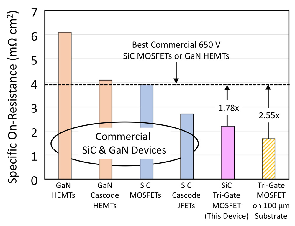
Figure 2: Specific on-resistance of commercial SiC and GaN devices, along with SiC tri-gate MOSFET and its expected performance enhancement from 100μm wafer thinning.
This work also allowed the inversion electron mobility to be estimated at 21, 13 and 10cm2/V-s for the upper fin surfaces and the trench bottoms and sidewalls, respectively. The researchers comment: “The MOS properties of the etched sidewalls clearly need to be optimized, and considerable room exists for improvement.”
The team adds: “Looking to the future, we can expect further performance improvement when the MOS interface on the trench sidewalls is optimized, since measured inversion mobility on a- and m-face epilayers is reported to be ~8x higher than the mobility on the sidewalls of our etched trenches”
https://doi.org/10.1109/LED.2020.3040239
The author Mike Cooke is a freelance technology journalist who has worked in the semiconductor and advanced technology sectors since 1997.


