


News: Microelectronics
18 December 2020
Leti highlights progress in GaN power electronics
Micro/nanotechnology R&D center CEA-Leti of Grenoble, France says that two complementary research papers presented at the 66th IEEE International Electron Devices Meeting (IEDM 2020) confirm that its approach to gallium nitride (GaN) technologies is on track to overcome challenges in the architecture and performance of advanced GaN devices embedding a MOS gate, and targeting the fast-growing global market for power-conversion systems.
Researchers recounted experiments with variations of high-electron-mobility transistors (HEMTs) based on GaN-on-silicon (GaN-on-Si). Compared with silicon, GaN-based semiconductors improve both performance and reliability of increasingly compact power converters, and AlGaN/GaN HEMTs have shown the potential to replace power-conversion solutions based on silicon or silicon carbide (SiC) for high-frequency applications with high power and low noise. This technology is therefore expected to be a cost-effective power-conversion solution for many end-user applications, ranging from smartphones to kitchen appliances and e-vehicles and from battery loaders to DC/DC or AC/DC converters.
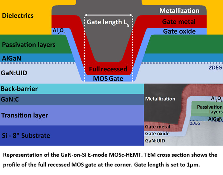
Considered together, the two papers provide a novel understanding of the gate stack of the GaN MOS-c HEMT developed at CEA-Leti in the IRT Nanoelec framework. They demonstrate the complexity of GaN MOS stack characterization as well as the requirement for deep expertise to report and analyze reliable parameter values. The work presented in these papers will also help to solve detrimental effects occurring in GaN devices to improve reliability, which is one of CEA-Leti’s key missions during an industrial transfer.
‘Carbon-Related pBTI Degradation Mechanisms in GaN-on-Si E-Mode MOSc-HEMT’
The paper ‘Carbon-Related pBTI Degradation Mechanisms in GaN-on-Si E-Mode MOSc-HEMT’ investigated the physics behind positive-bias temperature instability (pBTI) effects that occur when transistor gates are positively biased, to determine the root cause of this effect and to minimize it.
“We showed that the instabilities of voltage threshold (Vth) under positive gate stress were caused by two populations of traps,” says Aby-Gaël Viey, an author of the paper. “The first is related to defects in the gate oxide, which is a known effect, and the second to the presence of carbon atoms in nitrogen sites in GaN at the gate interface, which was a discovery, thus confirming the conclusions presented at IEDM.”
Generally in MOS technology, where BTI is a common reliability test (e.g. Si/SiGe/Ge-based CMOS technologies), the root causes of Vth instabilities are related to oxide defects that can be charged or discharged by electrons or holes, depending on device type (n/p-MOS) and bias polarity. In the case of GaN MOS-c HEMTs, the epitaxial structure grown underneath the transistor is extremely complex and far from homogeneous.
This study also confirmed the conclusions of the work that CEA-Leti reported in a paper at IEDM 2019 (‘Investigation of nBTI degradation on GaN-on-Si E-mode MOSc-HEMT’) that showed that carbon in GaN-in-N [CN], which usually is introduced as a deep acceptor to create a semi-insulating GaN layer for breakdown-voltage management, is responsible for a part of the BTI instabilities along with the common oxide traps charging. The epitaxial structure is thus a great concern to reduce and minimize instabilities in GaN power devices.
“In addition, our more recent work demonstrated that it is possible to accurately model and predict these threshold voltage instabilities with great precision,” Viey says. “Indeed, the known model of capture emission time (CET) maps were used to confirm the presence of the two populations of traps and predict pBTI degradation (Vth shift) under a certain gate/temperature stress condition.”
‘A Novel Insight on Interface Traps Density (Dit) Extraction in GaN-on-Si MOS-c HEMT’
The study ‘A Novel Insight on Interface Traps Density (Dit) Extraction in GaN-on-Si MOS-c HEMT’ set out to characterize the oxide/GaN interface electrical quality to understand if the interface trap density of CEA-Leti’s gate stack was the main threshold voltage (Vth) contributor in GaN-on-Si MOS-c HEMTs, and to confirm the performance of the institute’s solution developed during 10 years of R&D.
Interface trap density (Dit) extraction extracts the density of interface defects that are electrically active at an oxide/semiconductor interface, as well as its distribution in terms of energy with the bandgap of the semiconductor. It is important because Vth is directly related to physical parameters such as metal-gate work function and doping of the semiconductor, which are easily adjustable, and to some defect-related parameters such as fixed or mobile charges in the oxide and interface state density. This density can dramatically influence Vth if the interface is not correctly passivated and processed.
In the case of GaN MOS-c HEMTs, the GaN is dry-etched before oxide deposition, and this aggressive process step can have a tremendous impact on the future oxide/GaN interface. Thus, having an accurate and reliable characterization technique of this interface is a requirement for developing and optimizing MOS-based GaN power devices. “For other industries or researchers, this kind of approach would help to assess the interface trap density,” says William Vandendaele, an author of the paper.
Vandendaele says that the next steps for CEA-Leti are to expand the teams’ understanding of gate-stack optimization of GaN MOSc HEMTs to minimize Dit values, and to transfer the best product, process and characterization methodology to the institute’s industrial partners in the IRT PowerGan program.
CEA-Leti says that it will pursue its GaN roadmap with further research on epitaxy, devices, passive components, co-integration and system architectures to develop a GaN technology that allows switching frequencies in the MHz range and power densities 10 times those of silicon — all using standard CMOS processes to keep costs down.
Part of this work was achieved in the framework of IRT Nanoelec.


