


- News
18 October 2019
Vertical gallium nitride light-emitting diodes on 4-inch silicon wafers
Researchers in China have integrated high-power, reliable vertical indium gallium nitride (InGaN) light-emitting diodes (LEDs) on 4-inch silicon substrates [Shengjun Zhou et al, Optics Express, vol27, pA1506, 2019]. The team from Wuhan University, Changchun Institute of Optics, Fine Mechanics and Physics, and Xiamen Changelight Co Ltd, used a number of measures to improve the performance of the final LEDs by reducing current crowding and protecting the device structure from humidity.
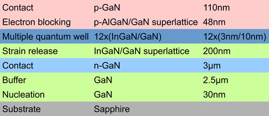
Figure 1: Vertical LED device layer MOCVD growth sequence.
The device layers were grown on patterned sapphire substrates using metal-organic chemical vapor deposition (MOCVD; see Figure 1). The LED fabrication began with inductively coupled plasma (ICP) etch into 1mmx1mm mesas for electrical isolation. A silicon dioxide (SiO2) current-blocking layer (CBL) was applied using plasma-enhanced CVD and patterning into 15μm-wide strips using photolithography and buffered-oxide wet etch (Figure 2).
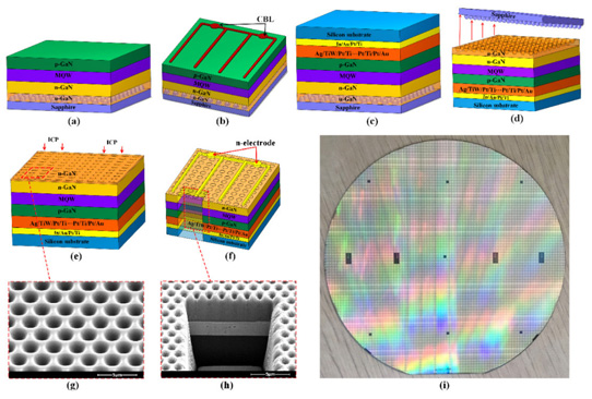
Figure 2: Fabrication process of LEDs: (a) MOCVD growth; (b) defining SiO2 CBL; (c) metal deposition and bonding to Si wafer; (d) laser lift-off (LLO) removal of sapphire substrate; (e) ICP etch to n-GaN contact; (f) deposition of p- and n- electrodes. (g) Scanning electron microscope (SEM) image of exposed n-GaN surface with hemispherical dimples after LLO and ICP etching. (h) Cross-sectional SEM image of LEDs bonded to Si wafer. (i) Photograph of LEDs on 4-inch Si wafer; colors arise from thin-film interference effects.
Ion-beam sputtering applied a 100nm silver film as reflector, followed by titanium/tungsten as a diffusion barrier. After electron-beam deposition of a platinum/titanium cap, rapid thermal annealing at 600°C was used to improve the GaN/silver ohmic contact.
The 4-inch-diameter p-Si final device substrate was prepared by adding multi-layers of titanium/platinum/gold and a titanium/platinum cap. A 2.5μm layer of indium was applied to the p-Si substrate before thermal compression bonding at 230°C. One feature of the titanium adhesion layer was that it also acted as a barrier against poisoning of the p-Si with gold. Platinum contamination of the p-Si was also avoided, according to energy-dispersive x-ray analysis.
A 248nm krypton-fluoride excimer laser was used to perform lift-off separation of the sapphire growth substrate. This was followed by ICP etch down to the n-GaN contact layer.
The n-GaN was treated with potassium hydroxide (KOH) or phosphoric acid (H3PO4) solution to texture the surface for improved light extraction. Chromium/platinum/gold was used to form the p- and n-electrodes for the LED. The n-contact metals were formed into 12μm-wide fingers.
The SiO2 CBL around the opaque electrodes directed current away from this region and made for more uniform current density in the light-emitting areas, according to simulations. Along with the vertical structure, it was hoped the CBL would reduce self-heating, making for more efficient performance over lateral structure devices. Current crowding increase leading to self-heating is a major problem in conventional lateral structure LEDs.
The vertical LED structure enabled much lower forward voltages for a given current injection – 2.87V at 350mA, compared with 3.52V with a conventional lateral LED structure (Figure 3). Lower forward voltage indicates lower input power and hence higher power efficiency. The light output power (LOP) for a given current injection was also higher in the vertical LED: lateral LED output saturated at ~320mA, while the vertical device increased in light power up to 1300mA. “The absence of premature LOP saturation in V-LEDs was attributed to reduced current crowding and enhanced heat dissipating compared to L-LEDs,” the team writes.
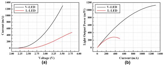
Figure 3: (a) Current-voltage profiles of lateral (L-) and vertical (V-)LEDs. (b) Light output power-current characteristics.
With 350mA, the vertical LED output power was 501mW, beating a previous report of a GaN vertical blue LED of ~450mW at the same injection. The researchers comment: “The higher LOP demonstrated in this work confirmed that integrating the optimized metallization scheme, SiO2 CBL and surface texturing by KOH wet etching is an effective approach to higher-performance V-LEDs.”
[I get a crude output/input power efficiency value of 50% (501mW/(2.87Vx350mA).]
The researchers also developed a platinum/titanium protective wrap-around layer for the silver/titanium-tungsten alloy structure. The wrap-around structure protected the mirror contact from humidity degradation. Operation at 85°C and 85% relative humidity degrade the performance of LEDs without lateral wrap-around protection over 1000 hours. By contrast, the LEDs with wrap-around platinum/titanium showed “negligible optical degradation even after an aging time of 1008h,” according to the researchers.
Vertical InGaN LEDs InGaN LEDs MOCVD Silicon substrates
https://doi.org/10.1364/OE.27.0A1506
The author Mike Cooke is a freelance technology journalist who has worked in the semiconductor and advanced technology sectors since 1997.


