


- News
24 May 2019
Pushing high-frequency transistor performance above 700GHz
Researchers based in South Korea and Japan claim record cut-off frequency performance for high-electron-mobility transistors (HEMTs) with channels constructed from indium gallium arsenide (InGaAs) quantum wells in indium aluminium arsenide (InAlAs) barriers [Hyeon-Bhin Jo et al, Appl. Phys. Express, vol12, p054006, 2019]. The team from Kyungpook National University and University of Ulsan in South Korea and NTT Device Technology Laboratories in Japan state: “To the best of our knowledge, this is the first demonstration of both fT and fmax in excess of 700GHz on any transistor on any material system.”
The researchers see such devices as potentially contributing to the ‘terahertz’ (300-3000GHz) radio-frequency (RF) electromagnetic (EM) sector, where the wavelength is in the sub-millimeter range. Such EM waves are or could be used in security/medical imaging systems, collision avoidance radars, next-generation transport communications, and wireless-local-area-networks (WLAN). Among the improvements of the researchers’ devices was reducing gate lengths to 25nm, boosting frequency performance.
The metal-organic chemical vapor deposition (MOCVD) epitaxial heterostructure was grown on 3-inch semi-insulating indium phosphide (InP) substrate. The layer sequence was 200nm In0.52Al0.48As buffer, 9nm InGaAs quantum well channel, 9nm In0.52Al0.48As barrier/spacer, 3nm InP etch stop, and 30nm heavily doped In0.52Al0.48As/In0.53Ga0.47As multi-layer cap.
The barrier/spacer layer was delta-doped with silicon. The cap was designed to reduce source/drain contact resistance. The channel layer had three components – 3nm In0.53Ga0.47As, 5nm In0.8Ga0.2As, and 1nm In0.53Ga0.47As. Hall measurements gave ~3x10¹²/cm2 two-dimensional electron gas density (2DEG) and mobility of 13,500cm2/V-s at 300K.
The epitaxial material was fabricated into HEMTs with recessed gates. The gate-to-channel distance was 5nm; the source-drain spacing was 0.8μm. The Ohmic source/drain contacts consisted of titanium/molybdenum/titanium/platinum/gold. The platinum/titanium/platinum/gold T-gates were formed with the help of silicon dioxide. Gate lengths as short as 25nm were achieved.
The 25nm-gate device had a DC on-resistance of 279Ω-μm, while the contact resistance was 40Ω-μm. The peak transconductance was 2.8mS/μm with the drain bias (VDS) at 0.8V. The subthreshold swing was 100mV/decade; the drain-induced barrier lowering (DIBL) was 120mV/V.
Measurements in the range 1-50GHz gave cut-off (fT) and maximum oscillation (fmax) frequencies of 703GHz and 820GHz, respectively, for 25nm-gate HEMTs with 2x20μm width (Figure 1). The drain and gate (VGS) biases were 0.5V and 0.15V, respectively. These offset values were chosen to put the HEMT near the peak transconductance state.
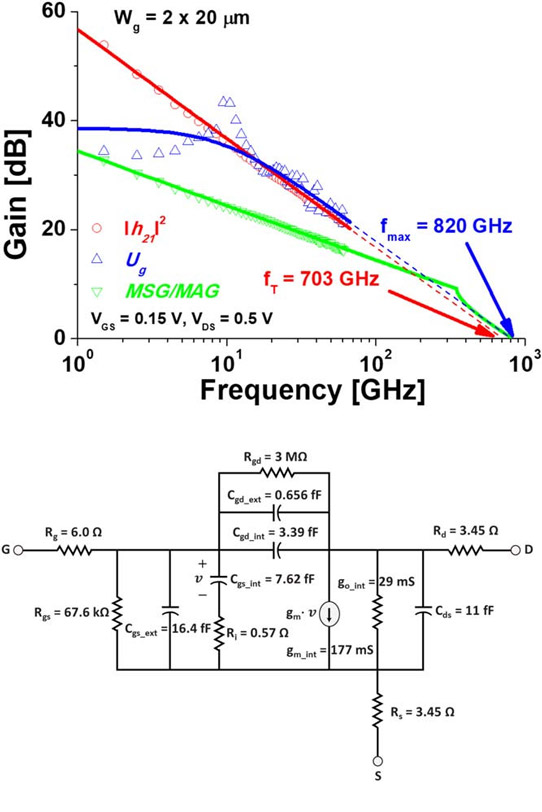
Figure 1: (a) Measured (symbols) and modeled RF gains (solid lines) (∣h21∣2, Ug, MSG and MAG), and (b) small-signal equivalent circuit model. Dashed lines represent least-squares projections from modeled ∣h21∣2 and Ug with −20 dB/decade fall-off.
There were problems in estimating fmax due to “sharp peaky behavior” of Mason’s unilateral power gain (Ug) with respect to frequency. The 820GHz fmax value was derived through a small-signal model from which a well-behaved gain parameter was extracted.
The researchers comment: “It is true that there exists inconsistency between the measured and the modeled Ug, especially in the low-frequency regime. This is due to the fact that our small-signal model did not take the effect of impact ionizations in the InGaAs QW channel into account. Nevertheless, this kind of the small-signal model has provided a reasonable estimate on fmax, since the effect of the impact-ionizations diminishes as the measured frequency goes over 10GHz.”
The small-signal model was also used to extrapolate the maximum stable gain (MSG) and maximum available gain (MAG) values. The fmax of 820GHz was also consistent with the MSG/MAG behavior. The fT value was derived from extrapolation of the short-circuit current-gain (∣h21∣2).
The team point out that the fT and fmax values above 700GHz were obtained using the same bias conditions, unlike in other reports on high-speed transistors.
Figure 2: Measured fT against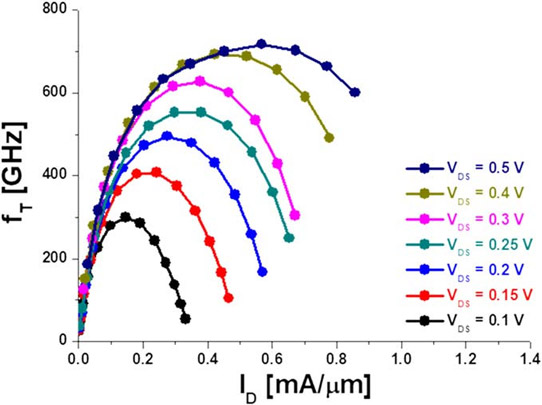 drain current (ID) with various VDS.
The researchers also studied the fT variation with drain current and bias (Figure 2). The team points out that at drain currents typical for low-noise amplifiers (0.1A/μm) the fT value was still more than 400GHz.
HEMTs InGaAs MOCVD InP substrate
https://doi.org/10.7567/1882-0786/ab1943
The author Mike Cooke is a freelance technology journalist who has worked in the semiconductor and advanced technology sectors since 1997.


