


- News
20 March 2019
Boosting extraction performance of ultraviolet light-emitting diodes
Researchers based in China have used thin-film and surface nanostructuring to boost the performance of ultraviolet (UV) light-emitting diodes (LEDs) by a factor of 3.9 [Chuanfei Ma et al, Nanotechnology, vol30 p185201, 2019].
The nanostructuring was performed on the thick aluminium gallium nitride (AlnGaN) n-side of the devices. This was enabled by flipping the LED material over onto another wafer and removing the silicon growth substrate. The nanostructuring was designed to reduce the total internal reflection that traps light due to the large contrast in refractive index between III-nitride materials (~2.4) and air (1). The light emission was from indium gallium nitride (InGaN) multiple quantum wells (MQWs).
The team at Suzhou Institute of Nano-Tech and Nano-Bionics and the University of Science and Technology of China grew the UV LED structure on silicon in the (111) crystal orientation. Metal-organic vapor phase epitaxy (MOVPE) deposited AlN/AlGaN as a multi-layer buffer, an n-AlGaN cladding layer, an InGaN/AlGaN pre-strained superlattice, InGaN quantum wells in AlGaN barriers, a p-AlGaN electron-blocking layer, a p-AlGaN current-spreading layer, and a p-GaN contact.
The epitaxial material was processed into vertical thin-film LED chips (Figure 1). The structure included an embedded n-contact and a silver-based reflective p-electrode. The embedded n-contact clears the ultimate emission surface from blockage by contact electrodes and pads.
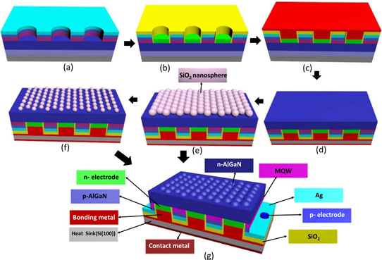
Figure 1: Schematic fabrication process: (a) deposition and patterning of silver-based reflective electrode with ICP-etched vias for embedded n-contact to n-AlGaN layer; (b) deposition of chromium/aluminium n-type contact metal and silicon dioxide (SiO2) insulating layer; (c) deposition of nickel/tin bonding metal and flipping onto silicon (100) wafer; (d) remove Si growth substrate and etch away AlGaN buffer layer, (e) SiO2 nanosphere single layer fabricated on N-face n-AlGaN, (f) tailored SiO2 nanosphere on N-face n-AlGaN, (g) AlGaN nanostructure (nanorod, nano-trapezoid, nanodome and nanocone) arrays on UV LED chips.
The nanostructuring of the nitrogen-face AlGaN was prepared with an oxygen-plasma treatment to convert the bonding from hydrophobic to hydrophilic for spin-coating of the SiO2 nanospheres to create a self-assembled array. Fluorine-based reactive ion etch was used to ‘tailor’ the sphere sizes to enable subsequent chlorine-based inductively coupled plasma (ICP) etch of the AlGaN surface into ‘nanodomes’. The nanospheres were removed with a buffered oxide etch, and dry etch damage of the nanodomes was smoothed with hydrochloric acid treatment.
The group performed ray-tracing Monte Carlo simulations and chose 250nm-diameter SiO2 nanospheres to create the domes. The simulations suggested an optimum height/diameter (H/D) ratio of 0.27, which gave a 68% light extraction efficiency, compared with 19% for a flat surface.
The current-voltage performance of LEDs with and without nanodomes was almost identical (Figure 2). The researchers point out that nanostructuring of the 2.5μm-thick n-AlGaN layer allows a large process window, in contrast to nanostructuring the thin ~100nm p-side of the device. Dry etching of the thin p-side layer carries risks of reducing conductivity, current spreading, etc. Further, such processing can also affect the underlying MQWs, reducing the efficiency of photon emission. Combined, one expects adverse effects on electrical and light-emission performance.
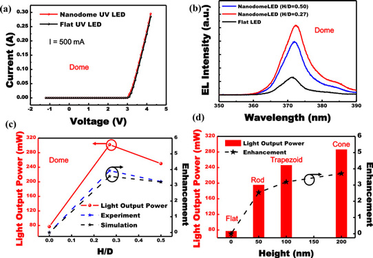
Figure 2: (a) Current-voltage curves of nanodome and flat UV LEDs, (b) electroluminescence spectra, (c) experimental and simulated light out power with various H/D nanodomes, (d) experimental light output power with nanorod, nano-trapezoid and nanocone arrays.
The integrated electroluminescence of the nanodome LEDs with 0.27 H/D ratio achieved 3.9x the performance of flat reference devices. Simulations suggested a 3.6x boost. The researchers also compared the performance of flat LEDs, against devices with ‘rod’, ‘trapezoid’ and ‘cone’ nanodome structures. The structures were achieved by not reducing the 250μm-diameter nanospheres with reactive ion etch and just performing the inductively coupled etch for different process times.
The researcher also examined the far-field radiation pattern and found that nanodomes cast the emissions more in the forward direction, compared with the flat LEDs. The researchers comment: “This phenomenon was more pronounced for the nanodome structure with H/D = 0.5, indicating that the nanostructures would facilitate the light extraction along the vertical direction, which is particularly useful to UV curing and other related applications of UV LEDs.”
The team adds that the AlGaN nanostructuring technique could easily be extended to deep UV vertical LEDs for enhancing light extraction.
https://doi.org/10.1088/1361-6528/aafd3d
The author Mike Cooke is a freelance technology journalist who has worked in the semiconductor and advanced technology sectors since 1997.


