


- News
24 October 2018
Large-area silicon carbide ultraviolet visible-blind avalanche photodiode
Hebei Semiconductor Research Institute in China has reported large-area 800μm-diameter 4H-polytype silicon carbide (SiC) ultraviolet (UV) avalanche photodiodes (APDs) with improved gain, quantum efficiency and dark current [Xingye Zhou et al, IEEE Electron Device Letters, published online 24 September 2018]. A variable-temperature photoresist reflow technique was used “for the first time” to create smooth beveled sidewalls that suppress leakage currents and avoid premature edge breakdown.
The researchers claim that, to the best of their knowledge, they have achieved the best overall performance for visible-blind UV detectors based on large-area 4H-SiC APDs in terms of high gain of more than 106, high quantum efficiency of 81.5%, low dark current and high UV/visible rejection ratio of 103.
UV detection covers a wide range of applications in astronomy, communications and biochemical analysis. UV is emitted in fluorescence experiments and by flames. Military warning and guidance systems can use visible-blind UV sensing to home in on or track missile plumes.
Up to now, SiC UV APDs have suffered from large dark current and premature breakdown under the larger reverse bias applied. This limits typical diameters to less than 250μm, reducing sensitivity. The researchers see their large-area devices as potential replacements for bulky, fragile and costly photomultiplier tubes.
The epitaxial structure consisted of 3μm heavily doped p-type (p+), 0.5μm lightly doped n-type multiplication (n-), 0.2μm n charge, 0.5μm n- adsorption, and 0.3μm n+ contact layers (Figure 1).
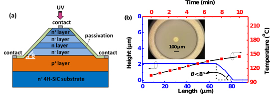
Figure 1: (a) Schematic cross section structure of 4H-SiC APDs; (b) temperature variation for photoresist reflow technique and profile of beveled mesa and (inset) top-view photo of 800μm-diameter 4H-SiC APD.
The fabrication began with inductively coupled plasma (ICP) mesa etching. The mesa was beveled to avoid edge breakdown effects. The thick photoresist for the mesa etch was subjected to a reflow process where the wafer was subjected to increasing temperature from 90°C to 145°C at a rate of 5°C/minute.
The variable temperature gives a smooth bevel surface, unlike fixed-temperature reflow at 145°C for 30 seconds, which results in saw-tooth patterns. A saw-tooth surface increases dark current and causes premature breakdown. The researchers suggest that fixed-temperature reflow creates a non-uniform thermal field with spatial variations in surface tension and reflow velocity for the photoresist, giving the observed surface roughness.
While the variable-temperature reflow gave consistent high breakdown values around 156V, measurements for APDs created using fixed-temperature reflow varied widely in the 100-150V range.
The further fabrication consisted of applying 200nm thermal oxide and 100nm plasma-enhanced chemical vapor deposition (PECVD) silicon nitride passivation, ICP and wet-chemical contact etching, electron-beam evaporation of nickel/titanium/aluminium/gold metal contacts, and 850°C metal contact annealing in nitrogen for three minutes. The completed device was 800μm diameter with the mesa bevel angle less than 8°.
Dark-current measurements with 140V and 150V reverse bias were carried out: the current was found to be quadratically dependent on the diameter, suggesting bulk leakage rather than surface leakage through the edge states. For the 800μm-diameter device the dark current was of the order 1pA (0.2nA/cm2) for low reverse bias.
Multiplication gain factors of more than 106 for 365nm ultraviolet were achieved over the ‘unity gain’ value at 10V reverse bias (Figure 2). Under a xenon lamp, the response with 140V reverse bias (4.2 gain) peaked at 0.18A/W for 274nm wavelengths. The corresponding external quantum efficiency was calculated to be 81.5%. The UV/visible rejection ratio was more than 103, given by the ratio of responses at 274nm and 400nm.
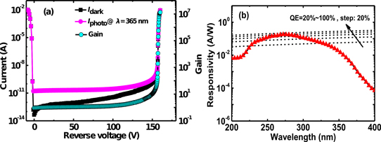
Figure 2: Ultraviolet detection performance of 800μm-diameter 4H-SiC APD: (a) current-voltage measurements and calculated multiplication gain; (b) spectral response corresponding to unity gain at reverse voltage of 140V.
The 800μm-diameter devices gave gain, quantum efficiency and dark-current performances comparable to that seen with much smaller APDs of less than 300μm diameter.
Silicon carbide ultraviolet avalanche photodiodes PECVD
https://doi.org/10.1109/LED.2018.2871798
The author Mike Cooke is a freelance technology journalist who has worked in the semiconductor and advanced technology sectors since 1997.


