


- News
25 July 2018
Plasmon-enhanced mid-infrared photodetection at room temperature
A team of researchers at Singapore’s Nanyang Technological University and Georgia State University in the USA, led by professor Dao Hua Zhang, have developed mid-wavelength infrared (MWIR, 3-5μm) photodetectors that operate at room temperature [Jinchao Tong et al, Appl. Phys. Lett., vol113, p011110, 2018]. The devices combine a two-dimensional subwavelength hole array (2DSHA) structure with an indium arsenide antimonide (InAsSb) n-i-p photodiode to boost detectivity while maintaining fast response.
MWIR detection is needed/desired in security, communication, medical diagnostics and remote sensing, but equipment often has to be cooled, increasing system complexity and expense in terms of capital investment and running costs. The researchers comment: “The realization of a room-temperature mid-wave infrared photodetector makes the application systems more economic and easily extended to more application domains.”
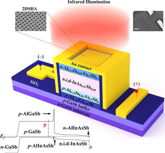
Figure 1: Design of 2DSHA-hetero n-i-p photodetector for enhanced MWIR photodetection. Inset: scanning electron micrographs of 2DSHA (left) and top view of 2DSHA-hetero n-i-p photodetector (at 30° angle), scale bars 1μm and 50μm, respectively. Left-bottom is a schematic band diagram of the heterojunction; p and n indicate positions of the metal electrodes.
The n-i-p part of the device was grown on tellurium-doped n-type gallium antimonide (n-GaSb) substrate. A 1μm intrinsic i-InAs0.91Sb0.09 absorber layer was placed between 20nm layers of n- and p-type aluminium indium arsenide antimonide (Al0.15In0.85As0.9Sb0.1) doped with silicon and beryllium, respectively.
The epitaxial structure began with a 1μm beryllium-doped p-GaSb contact/buffer, and 40nm of beryllium-doped p-Al0.42Ga0.58Sb as a wide-bandgap layer to block electrons forming a dark current on the p-side. At the same time, the p-Al0.15In0.85As0.9Sb0.1 layer limited type II electron-hole transitions from the absorber into the p-Al0.42Ga0.58Sb.
The device was fabricated with the aim of having the surface plasmon polaritons (SPPs) interact with the intrinsic absorber through the thin 20nm n-Al0.15In0.85As0.9Sb0.1. The top and bottom contacts consisted of 15nm of titanium (Ti) and 200nm of gold (Au). The square 300μm-side mesas were wet etched. The 350nm silicon dioxide (SiO2) passivation to protect the mesa and to reduce surface leakage was created using plasma-enhanced chemical vapor deposition (PECVD).
A gold-based two-dimensional subwavelength hole array (2DSHA) was fabricated using electron-beam lithography, metal evaporation and lift-off. The metal consisted of 3nm Ti adhesion and 70nm Au layers. The 70nm thickness for the Au layer exceeds the skin depth of 4.3-10.7nm for 1-6μm microwaves. This avoids direct transmission through the metal film.
In conventional p-i-n photodiodes there is a trade-off between responsivity and speed: thick intrinsic absorber layers are more responsive to optical radiation, but slower in tracking changes. The 2DSHA confines light near the metal-dielectric interface, allowing a thinner intrinsic layer to be used. The ‘dielectric’ in this case is the underlying semiconductor material.
The researchers estimate the surface plasmon resonance wavelength of their 2DSHA structure to be 3.5μm for the fundamental mode. This was aligned with the peak photocurrent response of the semiconductor heterostructure photodiode. The hole period of the 2DSHA was 900nm with the size of the square holes in the 2DSHA mesh being about half this. The team also explored other hole periods.
The 2DSHA with 900nm period showed the highest photocurrent at zero bias, in the wavelength range 2-5μm, over other 2DSHAs and over reference devices without 2DSHA. The enhancement over the reference for the 900nm-period structure was 3-4x.
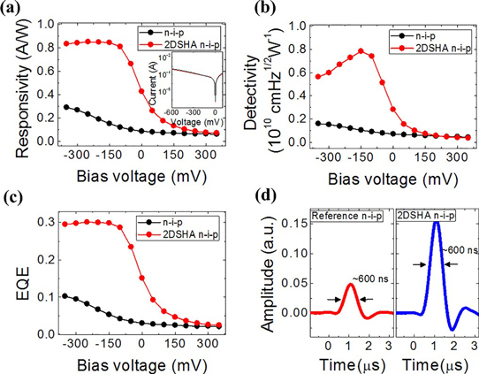
Figure 2: Room-temperature performance of 900nm-period 2DSHA-hetero n-i-p photodiode and reference. (a) Responsivity under biased voltages from -350mV to 350mV at room temperature. Inset: room-temperature current-voltage characteristics of photodiodes. (b) Blackbody detectivity. (c) External quantum efficiencies (EQE) at 3.5μm. (d) Impulse responses.
The device was also characterized using a 700°C blackbody source (Figure 2). The response saturated at around -150V reverse bias, giving a value of 0.85A/W, compared with 0.15A/W for a reference device without 2DHSA. The reference device had a higher response of 0.3A/W at -350V bias. The 2DSHA and reference devices had similar dark current levels.
The room-temperature blackbody detectivity was 0.80x10¹⁰cmHz1/2/W and 0.12x10¹⁰cmHz1/2/W for the 2DSHA and reference photodiodes, respectively. The external quantum efficiency at -150mV was ~30% for the 2DSHA device, about 5x that of the reference.
The speed of both devices was determined from the ~600ns-wide response from 200ns pulses of a 4.77μm quantum cascade laser. The researchers comment: “These measured results show that the performance of the 2DSHA-hetero n-i-p photodetector can be improved a lot without sacrifice of the speed.”
https://doi.org/10.1063/1.5018012
The author Mike Cooke is a freelance technology journalist who has worked in the semiconductor and advanced technology sectors since 1997.


