


- News
11 April 2018
Near-ultraviolet aluminium gallium nitride laser diode on silicon
Researchers in China claim the first observation of room-temperature electrically injected lasing in aluminium gallium nitride (AlGaN) near-ultraviolet (NUV) laser diodes (LDs) grown on silicon (Si) [Meixin Feng et al, ACS Photonics, vol5, p699, 2018].
The team from Suzhou Institute of Nano-Tech and Nano-Bionics, University of Science and Technology Beijing, University of Science and Technology of China, and Changchun Institute of Optics Fine Mechanics and Physics see prospects for laser microscopy, fluorescence spectroscopy, mass spectrometry, surface analysis, material processing, and laser lithography. Laser diodes offer compact, efficient, tunable alternatives to conventional gas and solid-state lasers at longer wavelength, and the researchers hope this can be extended into the NUV range. The use of silicon substrates should reduce costs through low material prices and the deployment of larger-diameter wafers.
The team reports that, while it has recently achieved visible electrically pumped lasing of III-nitrides on silicon, other groups have only managed optically pumped lasing.
Silicon substrates with (111) lattice orientation were processed with metal-organic chemical vapor deposition (MOCVD) to give a structure of an AlN/AlGaN multi-layer buffer, a 3.5μm n-Al0.03Ga0.97 contact, 150x 2.5nm/2.5nm n-Al0.2Ga0.8/n-GaN superlattice cladding, an 80nm n-GaN waveguide, 4x 2.5nm/10nm In0.05Ga0.95N/Al0.1Ga0.9N quantum well (QW)/barrier pairs, a 60nm GaN waveguide, a 20nm n-Al0.25Ga0.75 electron-blocking layer (EBL), 100x 2.5nm/2.5nm p-Al0.2Ga0.8/p-GaN superlattice cladding, and a 30nm p-GaN contact.
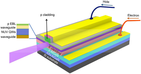
Figure 1: Schematic architecture of AlGaN-based NUV-LD directly grown on silicon.
Coplanar 4μmx800μm ridge-waveguide laser diodes were fabricated (Figure 1). The cleaved facets were coated with quarter-wave pairs of tantalum oxide/silicon dioxide dielectric. The front facet coating consisted of four pairs of layers, while the back facet had eight pairs. Facet coating reduced the laser threshold current from 550mA (17.2kA/cm2) to 350mA (10.9kA/cm2). The lasing was signalled by narrowing of the electroluminescence (EL) spectral linewidth, an elongated far-field pattern, and a discontinuity in the slope of light output power with current (Figure 2).
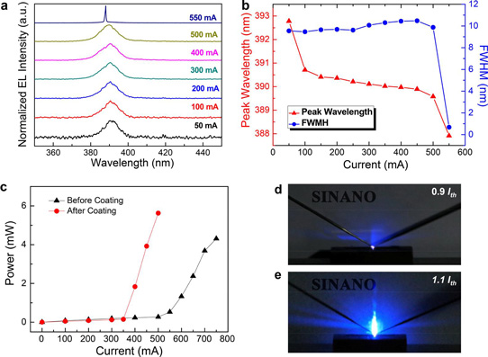
Figure 2: EL characteristics of as-fabricated AlGaN-based NUV-LD grown on silicon at room temperature. (a) EL spectra before cavity facet coating under various pulsed currents (400ns width, 10kHz repetition rate) – spectral resolution 0.1nm. (b) Peak wavelength and full-width at half maximum (FWHM) linewidth of laser diode before coating. (c) EL light output powers of laser diode before and after facet coating. Far-field patterns observed below (0.9x) (d) and above threshold current (1.1x) (e) as shown by blue fluorescence under NUV of white copying paper.
The researchers comment: “As compared with the reported value (~ 3kA/cm2) of NUV-LD grown on high-quality GaN substrates (TDD ~ 106cm-2) by epitaxial lateral overgrowth (ELOG), the threshold current density of the as-fabricated AlGaN-based NUV-LD grown on silicon was relatively high, which caused a limited lifetime (~ 1.5h) under a pulsed injection current of 450mA (pulse width of 400ns and a repetition rate of 10 kHz) at room temperature.”
The multi-layer buffer between the silicon substrate and device layers was designed both to compensate for tensile strain from the thermal expansion mismatch and cooling after growth, and to help prevent dislocations threading into the upper layers. The buffer structure consisted of steps from 300nm AlN nucleation, through 320nm Al0.35Ga0.65N and 450nm Al0.17Ga0.83N.
AlGaN Near-ultraviolet laser diodes Silicon substrates MOCVD
https://pubs.acs.org/doi/abs/10.1021/acsphotonics.7b01215
The author Mike Cooke is a freelance technology journalist who has worked in the semiconductor and advanced technology sectors since 1997.


