


- News
24 July 2017
Fujitsu achieves record output density with power amplifier for W-band GaN transmitters
At the 12th International Conference on Nitride Semiconductors (ICNS-12) in Strasbourg, France (24-28 July), Tokyo-based Fujitsu Ltd and Fujitsu Laboratories Ltd are announcing the development of a gallium nitride (GaN) high-electron-mobility transistor (HEMT) power amplifier for use in W-band (75-110GHz) transmissions. Part of the research was carried out with support from Innovative Science and Technology Initiative for Security, established by the Acquisition, Technology & Logistics Agency (ATLA), Japan Ministry of Defense.
To realize long-distance, high-capacity wireless communications, a promising approach is to utilize the W-band and other high-frequency bands that encompass a broad range of usable frequencies, and increase output with a transmission power amplifier. At the same time, demand exists for improved efficiency in power amplifiers in order to mitigate the increased power consumption of communication systems.
Fujitsu has now developed a power amplifier for use in W-band transmissions that offers both high output power and high efficiency, improving transistor performance through the reduction of electrical current leakage and internal GaN-HEMT resistance. Fujitsu has achieved record output power density in the W-band of 4.5W per millimeter of gate width, and has confirmed a 26% reduction in energy consumption compared with conventional technology.
Development background
Wireless data traffic from mobile communications has increased dramatically over the last few years, and with the spread of 5G and Internet of Things (IoT) devices, it is predicted to increase at an annual growth rate of 1.5 times until the year 2020. To build this sort of high-capacity next-generation wireless communications network, attention has been focused on wireless communication technology using the high-frequency W-band. The range of frequencies that can be used in the W-band is very broad and, because communication speed can be rapidly increased in this band, it is well suited to this kind of high-bandwidth wireless communication, says Fujitsu.
Conventional wireless communications technology has allowed for performance of several Gbit/s over distances of several kilometers, but achieving an even greater increase in wireless communication distance and capacity utilizing the W-band demands further increases to the output of power amplifiers to boost signals during transmission.
To increase distance and capacity, it is necessary to expand the frequency bandwidth that can be amplified while simultaneously supporting modulation methods that can transmit more information within the same frequency bandwidth, and a strong requirement is to have less distortion when the signal is amplified. Another aim is to keep in check the energy consumption of communication systems that accompanies greater distances and capacities, along with improved energy efficiency in power amplifiers.
To both increase the distance and capacity of wireless communications and decrease energy consumption with indium aluminium gallium nitride (InAlGaN) HEMTs, Fujitsu has developed two technologies that effectively reduce internal resistance and current leakage.
1. Technology to reduce internal resistance
Fujitsu has developed device technology that can reliably reduce resistance to one tenth that of previous technology when current flows between the source or drain electrodes and the GaN-HEMT device. The technology uses a manufacturing process that embeds GaN plugs directly below the source and drain electrodes, which generate electrons at high densities (Figure 1).
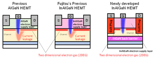
Figure 1: Schematic cross-sectional view of GaN-HEMT device structure.
It is necessary to transport the electrons that come from the source electrode to the two-dimensional electron gas (2DEG) field as smoothly as possible. The structure of the previous technology causes the electron supply layer to become a barrier, however, and internal resistance increases between the source electrode and the two-dimensional electron gas. By applying this new technology, Fujitsu can run high currents through the transistor with significantly less resistance (Figure 2).
2. Technology to control current leakage
Current leakage occurs when the two-dimensional electron gas (which moves at high speed on the boundary at the top of the channel layer) takes a detour below the gate when the transistor is in its off-state. This leakage causes deterioration in the operational performance of the power amplifier. Normally, it is possible to reduce current leakage by placing a barrier layer beneath the channel layer, but in that case the amount of two-dimensional electron gas also decreases, reducing the drain current.
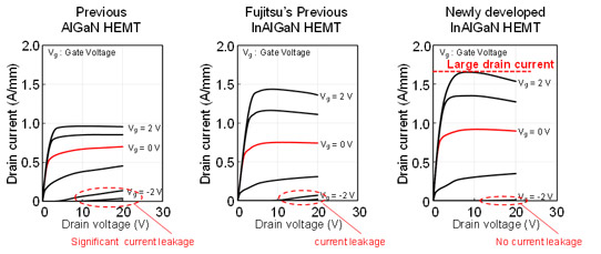
Figure 2: Comparison of transistor characteristics.
The new technology maintains high drain currents by effectively distributing indium gallium nitride (InGaN) to create a barrier layer below the channel layer. This reduces electron detours during operation, successfully providing significant reductions in current leakage (Figures 1 and 2).
Performance
The previous record for power amplifier output density in the W-band for transmitters was 3.6W per millimeter of gate width (with technology developed by Fujitsu Laboratories). This has improved significantly with the newly developed technology, which delivers power output of 4.5W per millimeter of gate width for a power amplifier designed to operate at 94GHz. In addition, the new technology achieved a reduction in energy consumption of 26% compared to the previous technology through a reduction in current leakage.
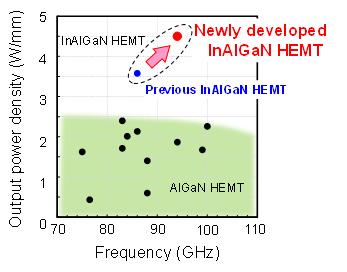 Figure 3: Comparison of GaN-HEMT power amplifier performance.
Fujitsu expects that the use of this power amplifier will allow the achievement of high-capacity, long-distance wireless communications between two connected systems at different locations at over 10Gbit/s and at distances greater than 10km.
Future plans
Fujitsu aims to apply this technology broadly to the development of power amplifiers for purposes calling for wireless communications that offer long range and higher capacity, while offering easier installation than fiber optics. The goal is to commercialize the new technology in high-speed wireless communication systems by 2020, and employ it in situations such as a method of restoring communications when fiber-optic cables have been severed by natural disasters or as a way of setting up temporary communications infrastructure when holding events.
Fujitsu develops GaN power amplifier with record output for W-band wireless transmission
www.fujitsu.com/jp/group/labs/en


