- News
9 November 2016
Fraunhofer ISE and EVG set 30.2% efficiency record for silicon-based multi-junction solar cell
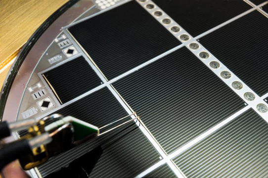
Researchers at the Fraunhofer Institute for Solar Energy Systems (ISE) in Freiburg, Germany together with EV Group of St Florian, Austria - a supplier of wafer bonding and lithography equipment for semiconductor, micro-electro-mechanical systems (MEMS), compound semiconductors, power devices and nanotechnology applications - have fabricated a silicon-based multi-junction solar cell with two contacts and a solar energy conversion efficiency exceeding the theoretical limit of silicon solar cells.
The researchers used a direct wafer bonding process to transfer a few microns of III-V semiconductor material to silicon. After plasma activation, the subcell surfaces are bonded together in vacuum by applying pressure. The atoms on the surface of the III-V subcell form bonds with the silicon atoms, creating a monolithic device.

Picture:Wafer-bonded III-V/Si multi-junction solar cell with 30.2% efficiency ©Fraunhofer ISE/A. Wekkeli.
The researchers say that the efficiency achieved presents a first-time result for this type of fully integrated silicon-based multi-junction solar cell. The complexity of its inner structure is not evident from its outer appearance: the cell has a simple front and rear contact - just like a conventional silicon solar cell - and therefore can be integrated into photovoltaic modules in the same manner.
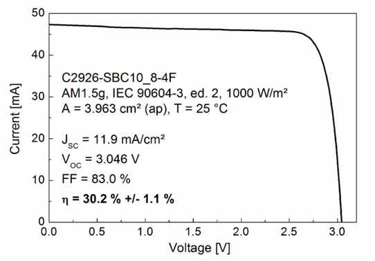
"We are working on methods to surpass the theoretical limits of silicon solar cells," says Dr Frank Dimroth, head of Fraunhofer ISE's III-V Epitaxy and Solar Cells department. "It is our long-standing experience with silicon and III-V technologies that has enabled us to reach this milestone." A conversion efficiency of 30.2% for the III-V/Si multi-junction solar cell of 4cm2 was measured at Fraunhofer ISE's calibration laboratory. In comparison, the highest efficiency measured to date for a pure silicon solar cell is 26.3%, and the theoretical efficiency limit is 29.4%.

Picture: Current-voltage characteristic of the GaInP/GaAs/Si solar cell, measured at the Fraunhofer ISE calibration laboratory.
The III-V/Si multi-junction solar cell consists of a sequence of subcells stacked on top of each other. Such tunnel diodes internally connect the three subcells made of gallium indium phosphide (GaInP), gallium arsenide (GaAs) and silicon (Si), which span the absorption range of the sun's spectrum. The GaInP top cell absorbs radiation between 300 and 670nm. The middle GaAs subcell absorbs radiation between 500 and 890nm and the bottom Si subcell between 650 and 1180nm, respectively. The III-V layers are first epitaxially deposited on a GaAs substrate and then bonded to a silicon solar cell structure. Subsequently, the GaAs substrate is removed, and a front and rear contact as well as an anti-reflection coating are applied.
"Key to the success was to find a manufacturing process for silicon solar cells that produces a smooth and highly doped surface which is suitable for wafer bonding as well as accounts for the different needs of silicon and the applied III-V semiconductors," says Dr Jan Benick, team leader at Fraunhofer ISE. "In developing the process, we relied on our decades of research experience in the development of highest-efficiency silicon solar cells," he adds.
"With this achievement, we have opened the door for further efficiency improvements for cells based on the long-proven silicon material," says ISE's director professor Eicke Weber, regarding breaking the "glass ceiling" of 30% efficiency with a fully integrated two-contact silicon-based solar cell.
"The III-V/Si multi-junction solar cell is an impressive demonstration of the possibilities of our ComBond cluster for resistance-free bonding of different semiconductors without the use of adhesives," says Markus Wimplinger, corporate technology development & IP director at EVG. "Since 2012, we have been working closely with Fraunhofer ISE on this development." The direct wafer-bonding process is already used in the microelectronics industry to manufacture computer chips.
On the way to the industrial manufacturing of III-V/Si multi-junction solar cells, the costs of the III-V epitaxy and the connecting technology with silicon must be reduced. There are still great challenges to overcome in this area, which Fraunhofer ISE aims to solve through future investigations. Its new Center for High Efficiency Solar Cells (currently being constructed in Freiburg) will provide facilities for developing next-generation III-V and silicon solar cell technologies. The ultimate objective is to make high-efficiency solar PV modules with efficiencies of over 30% possible in the future.
The young researcher Dr Romain Cariou carried out research on this project at Fraunhofer ISE with the support of a Marie Curie Postdoctoral Fellowship. Funding was provided by the European Union project HISTORIC. The work at EVG was supported by the Austrian Ministry for Technology.
Fraunhofer ISE teams with EVG to enable direct wafer bonding for next-gen solar cells
EVG extends wafer bonding equipment and process solutions for covalent bonding technology
EV Group Fraunhofer ISE III-V multi-junction solar cells


