


- News
22 April 2015
Indium gallium arsenide on insulator transistors with buried yttrium oxide
Korea Institute of Science and Technology has presented what it says is the first demonstration of indium gallium arsenide on-insulator (In0.53Ga0.47As-OI) transistors with a buried yttrium oxide (Y2O3 BOX) layer [SangHyeon Kim et al, IEEE Electron Device Letters, published online 31 March 2015].
The researchers see InGaAs-OI as a promising alternative to more complicated tri-gate devices. The use of Y2O3 should enable reduced equivalent oxide thickness (EOT) compared with aluminium oxide, on the basis of a higher dielectric constant (16 versus 9-12). Reduced EOT brings the gate effectively closer to the channel, improving electrostatic control.
A simple metal-oxide-semiconductor (MOS) back-gate stack transistor was constructed by layer transfer of InGaAs from its indium phosphide (InP) growth substrate to silicon with a Y2O3 buried layer (Figure 1). The InGaAs surface was prepared by native oxide removal and passivation with acetone, ammonium hydroxide, ammonium sulfide solutions. The clean surface was covered with 10nm of Y2O3 produced through electron-beam evaporation. The silicon target substrate was also covered with 10nm Y2O3, after cleaning with hydrofluoric acid.
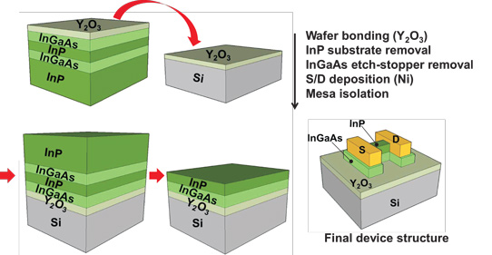
Figure 1: Fabrication process for InGaAs-OI on silicon wafer by direct wafer bonding and schematic of final device.
The wafer bonding was achieved with hand pressure in air. The InP growth substrate and an InGaAs sacrificial layer were removed with hydrochloric and phosphoric acid wet etching. Nickel/gold was used for the source and drain electrodes. An InP etch-stop layer was selectively removed from the source and drain areas, but left in place over the channel region to reduce surface effects, which can impact effective mobility.
The final device was subjected to rapid thermal annealing at 300°C. The gate length was 2μm and the body (channel) thickness was 10nm. The subthreshold swing was 90mV/decade, described by the researchers as "very low" in view of the relatively large EOT.
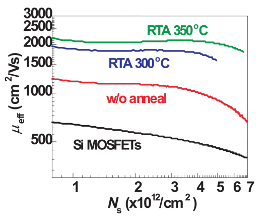
Figure 2: Effective mobility (μeff) characteristics of InGaAs-OI transistors produced with various annealing temperatures.
The effective mobility was enhanced by a factor 2.5x over the value for silicon-based devices, even without annealing (Figure 2). Annealing at 300°C increased the effective mobility to 2000cm2/V-s. These first results should be improvable with process optimization, according to the researchers.
The interface trap density extracted from the subthreshold behavior was 1.1x10¹²/eV-cm2, comparable with values from MOS capacitor measurements. These capacitor structures were produced on InGaAs/InP substrates with 10nm Y2O3 dielectric and top and bottom electrodes of platinum/gold and nickel/germanium/gold, respectively. Post-metal annealing at 350°C reduced interface the trap densities to as low as 4x10¹²/eV-cm2 near the conduction-band edge, according to capacitance-voltage measurements. The hysteresis was 15mV.
InGaAs InP substrate Metal oxide semiconductor back-gate stack transistor
http://ieeexplore.ieee.org/xpl/login.jsp?tp=&arnumber=7073604
The author Mike Cooke is a freelance technology journalist who has worked in the semiconductor and advanced technology sectors since 1997.


