


- News
1 October 2013
PVA TePla launches modular, highly automated PVT system for SiC crystal mass production
PVA TePla of Wettenberg, Germany has launched the baSiC-T physical vapor transport (PVT) crystal growth system (which uses sublimation of a source powder at high temperatures) for the mass production of silicon carbide (SiC) material.
Typical applications of SiC crystal include high-performance electronics for end-markets such as hybrid and electric cars and air-conditioning systems, as well as optoelectronics applications such as LEDs and DC/AC converters for photovoltaics. The major advantage of silicon carbide material lies in the energy-saving potential of over 40% compared with conventional silicon components, says the firm. In addition, SiC can also be used at high temperatures and high voltages in excess of 10,000V, dramatically exceeding the potential of silicon.
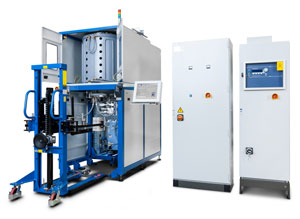 PVA TePla’s new baSiC-T system.
PVA TePla says that the design of the baSiC-T system is based on a modular concept and allows the use of substrates (seeds) with a diameter ranging from 100mm to 150mm. Low operating costs and a high degree of automation facilitate inexpensive mass production of silicon carbide, the firm claims.
Systems for manufacturing SiC crystal have already been delivered to several customers in Europe and Asia, and successfully accepted, providing proof of the systems’ performance, the firm claims.
In addition to the baSiC-T, a series of other PVA TePla systems are already being used in the field of power electronics. The SiCube is an industrially tested system for SiC crystal mass production by means of PVT and high-temperature chemical vapor deposition (HTCVD). The Floatzone (FZ35) and Czochralski (EKZ) systems are used to crystallize high-purity silicon. The recycling of susceptors used in gallium nitride (GaN) epitaxy processes is performed in special PVA TePla vacuum furnaces. Also available are various metrology technologies for non-destructive quality control.
www.pvatepla.com/en/products/crystal-growing-systems


