


- News
18 June 2013
First yellow LEDs from nitride semiconductor MQWs on silicon
Hong Kong University of Science and Technology (HKUST) has developed silicon substrate growth of high-performance nitride semiconductor light-emitting diodes (LEDs) in the green and yellow bands [Xinbo Zou et al, IEEE TRANSACTIONS ON ELECTRON DEVICES, published online 29 May 2013]. The researchers claim the 565nm yellow LEDs as the first multi-quantum well (MQW) devices produced on silicon.
Producing longer-wavelength nitride semiconductor LEDs is challenging due to the difficulty of producing good-quality indium gallium nitride (InGaN) with higher indium concentration. Although growth on silicon is well established in nitride semiconductor transistor development, it is only fairly recently that similar growth methods have been applied to LED device material.
The attractions of silicon as a substrate include lower material cost and economies of scale in mass production from the larger wafer diameters available. However, the quality of nitride semiconductors on silicon suffer from the larger lattice mismatch compared with conventional, more expensive substrates of free-standing GaN, sapphire or silicon carbide (SiC).
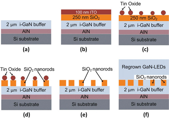
Figure 1: Schematic process for GaN-based LEDs with embedded SiO2 nanorods: (a) 2μm GaN deposition on Si; (b) SiO2 and ITO deposition; (c) ITO patterning in HCl; (d) SiO2 dry etching; (e) dry etching mask removal; and (f) re-growth of GaN-based LEDs.
The initial template, grown on 2-inch (111) silicon using metal-organic chemical vapor deposition (MOCVD), consisted of aluminium nitride (AlN) nucleation, 8 pairs of aluminium nitride/gallium nitride (AlN/GaN) layers to create a superlattice (SL) as stress-balancing interlayer, and a 2μm GaN buffer.
Silicon dioxide (SiO2) nanorods were then formed by depositing layers of SiO2 and indium tin oxide (ITO), etching the ITO with hydrochloric (HCL) acid solution to form a mask, and finally plasma etching out the nanorods. The density of nanorods was 2x10⁹/cm2, giving a surface coverage of 35%. The purpose of the nanorods was to act as a mask in GaN re-growth with reduced dislocation density and improved crystalline quality.
The LED structure was then grown by MOCVD with re-growth of 800nm of GaN around the nanorods, an AlN/GaN SL interlayer, 2μm of n-type GaN, a 5-period multiple quantum well (MQW), and 200nm of p-GaN. The re-grown GaN had a dislocation density of 8x10⁸/cm2, described by the researchers as “one of the lowest values reported for GaN-on-Si substrates, as determined by TEM”.
Materials suitable for emitting yellow (565nm) and green (505 and 530nm) light were prepared and formed into 300μm x 300μm LED chips.
As was to be expected, the light output power (LOP) decreased as the wavelength increased (Figure 2). At 20mA, the output at 505nm was 1.18mW. The respective values for 530nm and 565nm were 0.30mW and 74μW, respectively. Saturation of the light output power was achieved at 7.60mW (200mA), 2.72mW (180mA) and 0.52mW (160mA), for the 505nm, 530nm and 565nm devices, respectively.
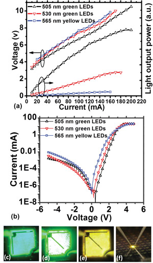 Figure 2: (a) Light output power and voltage versus current characteristics of green and yellow LEDs encapsulated with silicone domes. (b) Current versus voltage characteristics. Light-emitting images of (c) 505nm, (d) 530nm and (e, f) 565nm LEDs.
The researchers comment: “This is the first report of fabricated 565nm yellow InGaN/GaN MQW LEDs on a silicon substrate, and the LOP of the 505nm LEDs was much higher than that for the LEDs on Si reported in the past.”
Apart from the improved material quality, the researchers believe that the nanorods also provide a scattering enhancement of light extraction from the devices.
The longer wavelength also increased the forward voltage at 20mA from 3.8V at 505nm to 4.3V at 565nm. Higher forward voltages indicate larger power losses. The researchers attribute the two primary reasons for the lower performance of the longer-wavelength devices as “inferior p-GaN quality induced by the lower growth temperature and the lattice mismatch introduced by the high-indium-content quantum wells”.
Temperature-dependent photoluminescence and electroluminescence spectra indicated the presence of In-rich clusters that induced localized states in the MQWs. Effective carrier injection into these localized states played a key role in the highly efficient ‘green gap’ spectrum emission, the researchers believe.
Yellow LEDs MQWs on silicon GaN AlN MOCVD
http://ieeexplore.ieee.org/xpl/articleDetails.jsp?arnumber=6521369
The author Mike Cooke is a freelance technology journalist who has worked in the semiconductor and advanced technology sectors since 1997.
