


- News
5 July 2013
First 40GHz results for quaternary nitride semiconductor HEMTs
Researchers based in France and Germany report the first power characterization of ‘quaternary’ indium aluminium gallium nitride (InAlGaN) high-electron-mobility transistors (HEMTs) at 40GHz [F. Lecourt et al, IEEE Electron Device Letters, published online 19 June 2013]. The participating bodies were Lille University’s Institut d’Electronique, Microélectronique et Nanotechnologie (IEMN), RWTH Aachen University, and Aixtron SE.
It is hoped that quaternary devices, which can be grown with lattice-matched layers, will lead to reduced defect densities and thus improved reliability.
The epitaxial material was grown on c-plane sapphire using an Aixtron 3x3-inch CCS metal-organic chemical vapor deposition (MOCVD) reactor. The layer structure consisted of a 500nm AlN nucleation layer, 400nm of Al0.24Ga0.76N, a 3.5μm GaN buffer layer, a 1nm AlN mobility enhancer, and a 8.3nm In0.11Al0.72Ga0.17N barrier layer.
Hall measurements on this material gave a carrier concentration of 1.2x10¹³/cm2 and mobility of 2200cm2/V-s, resulting in 240Ω sheet resistance. The researchers claim the very high mobility as “the highest value ever reported on In-containing GaN-based HEMTs”.
The transistors were produced with rapid thermal annealed titanium/aluminium/nickel/gold ohmic source-drain contacts and nickel/gold T-gates. Devices with gate lengths of 75nm and 225nm were fabricated. The transistors were passivated with silicon nitride, applied using plasma-enhanced chemical vapor deposition (PECVD).
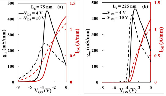
Figure 1: Transfer characteristics at 4V (solid line) and 10V (dotted line) drain biases for devices with 75nm (a) and 225nm (b) gate length.
The maximum channel current density (Figure 1) for both gate lengths at a 4V drain voltage was 1.4A/mm at 2V gate (1.25A/mm at 0V). The channel current is reduced with the higher drain bias of 10V – it is thought that this is due to thermal effects. The peak extrinsic transconductance was 450mS/mm at 4V drain bias, but only 250mS/mm at 10V, for the shorter gate length of 75nm. The 225nm-gate HEMT has a transconductance greater than 400mS/mm at 10V.
The pinch-off gate potential of the long-gate device was -4V at both drain bias values. However, the short-gate HEMT had a pinch-off of -4.5V for 4V drain and -9V for 10V drain. “These degradations can be attributed to short-channel effects due to a lower aspect ratio between the gate length and the barrier layer thickness,” the researchers comment.
The gate leakage of the devices was around 100μA/mm up to 10V drain bias.
Frequency performance measurements gave a cut-off (fT) of 113GHz and power-gain cut-off (fmax) of 200GHz for a 75nm-gate-length device with 2x50μm width at the peak transconductance point for 4V drain bias. “To our knowledge, these results represent the highest performance for AlInGaN HEMT technology with T-shaped gate transistors,” the researchers remark, comparing with a 220GHz/60GHz fT/fmax 66nm-gate-length device reported by University of Notre Dame (USA) in 2011.
Under the same bias conditions the larger-gate IEMN device managed an fT of 60GHz and fmax of 120GHz. The fT value degraded at 10V drain, moving down from 113GHz to 76GHz for the short-gate HEMT and from 60GHz to 55GHz for the long-gate device.
The researchers traced the cause of these performance degradation effects as being due to increased drain delay in the short-gate devices. “This is physically related to the increase of the output conductance gd for higher drain biases due to the presence of short channel effects,” they write.
Current collapse was investigated with pulsed measurements. The current drop for long-gate devices was 12% for gate lag and 27% for drain lag conditions. The respective results for the short-gate HEMT were 15% and 39%. The worse collapse here was attributed to the higher peak electric field for the shorter gate, increasing charge trapping.
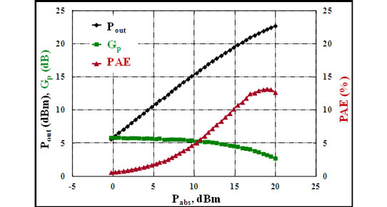
Figure 2: Microwave power characteristics at 40GHz for 2x50μm AlInGaN/GaN HEMT on sapphire substrate with 225nm gate length.
The output power density for the long-gate HEMT at 40GHz was 2W/mm with 13% power-added efficiency (PAE) and 6dB linear power gain (Figure 2). A previous effort with InAlGaN-barrier HEMTs by the Fraunhofer Institute in Germany reported 10GHz power density results of 5.6W/mm (PAE 31%) with a quaternary device in 2010.
Ternary AlGaN/GaN devices on silicon at 40GHz achieving an output power density of 3.3W/mm (20.1% PAE) were reported earlier this year by an IEMN-led team. According to the French/German paper, the record power density of 10.5W/mm (34% PAE) at 40GHz is held by a 2005 report of an AlGaN device on expensive silicon carbide from University of California Santa Barbara.
The shorter-gate device managed a 1.25W/mm density “due to the combination of high current drop under drain lag condition and short-channel effects”. The performance could be improved using a better thermal conductor as a substrate, such as silicon or silicon carbide, the researchers believe.
The researchers add: “The addition of a back barrier or an AlGaN buffer could also lead to better performances through a better electron confinement. Additionally, further investigations should be focused on surface state passivation to reduce parasitic lag effects.”
http://ieeexplore.ieee.org/xpl/articleDetails.jsp?arnumber=6544248
The author Mike Cooke is a freelance technology journalist who has worked in the semiconductor and advanced technology sectors since 1997.
