- News
6 September 2012
Layer insertion to avoid nitride LED efficiency droop
Taiwan researchers have achieved a reduction in luminous efficiency droop from 42% to 7% by inserting p-type indium gallium nitride (p-InGaN) between the active light-emitting and electron-blocking layers of a nitride semiconductor light-emitting diode (LED) [Ray-Ming Lin et al, Appl. Phys. Lett., vol101, p081120, 2012]. The researchers were based at Chang Gung University, National Cheng Kung University, and MOME Business Development Group (LED Division).
Nitride semiconductor LEDs are being developed for white light applications such as liquid-crystal display backlights and general illumination. These devices suffer from a degradation in efficiency at higher currents. Researchers have tried various methods to overcome this to allow higher-efficiency operation of these devices at higher currents. Solving the problem would enable wider use of LEDs at lower cost both through more efficient operation and the need for fewer devices in a module.
The researchers see their p-InGaN insertion as a way to overcome the asymmetry between electron and hole transport in nitride LEDs. While electrons often flow beyond the active region of the device into the p-contact, holes barely make it beyond the first well. The electron overflow reduces efficiency by reducing the number of holes available for injection into the active region. Nitride LEDs frequently have an electron-blocking region of aluminium gallium nitride (AlGaN) to reduce the electron overflow, but this then further impedes the flow of holes.
The Taiwan InGaN-based blue LEDs were produced from material grown on c-plane sapphire with an SR2000 metal-organic chemical vapor deposition (MOCVD) reactor supplied by Taiyo Nippon Sanso. The layer sequence consisted of a 25nm GaN nucleation layer, a 1μm undoped GaN buffer, 3μm of Si-doped n-GaN, two pairs of 3nm InGaN (10%-In) and 12nm GaN strain relaxation layers, a multi-quantum well (MQW) of four pairs of 3nm InGaN (16%-In) wells and 12nm GaN barriers followed by a 3nm last well and 3nm last barrier, 5nm of GaN, an InGaN (7%-In) or p-InGaN insertion layer, a 20nm p-AlGaN (20%-Al) electron-blocking layer, and a 100nm p-GaN contact. The active region was designed to emit 440nm wavelength blue light. The LEDs were formed from 1mm x 1mm chips of the material.
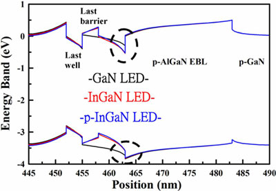 Figure 1. Calculated band diagrams for GaN, InGaN, and p-InGaN LEDs at a forward current of 20mA.
Based on simulations (Figure 1), the researchers believe that the effect of the InGaN insertion is to block electron overflow and increase hole injection into the LED structure, increasing external quantum efficiency (EQE). By doping InGaN as p-type, there is also a benefit resulting from a lower activation energy for hole generation compared with p-GaN. The simulation suggested a reduction of almost three orders of magnitude in electron overflow and more than one order of magnitude increase in hole concentration in the last well when LEDs with p-InGaN insertion were operated at 1A injection current.
Processed devices were tested at a current of up to 1A using a 700μsec, 0.1% duty-cycle pulsed signal to avoid self-heating effects (Figure 2). The undoped InGaN insert provided the highest peak efficiency and a slight mitigation of the droop effect. The researchers comment: “We attribute this improvement to the enhanced hole injection efficiency and greater retardation of electron overflow as a result of the bandgap energy of In0.07GaN being lower than that of GaN.”
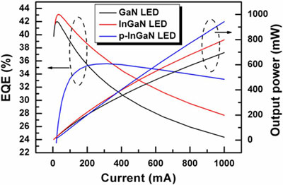 Figure 2. External quantum efficiencies (EQEs) and output powers of GaN, InGaN, and p-InGaN LEDs plotted with respect to forward current.
The p-doping of the InGaN insert reduced the peak while pushing it out to a higher current of around 316mA. The efficiency droop at 1A was 7% compared with the peak. The droop of the conventional device was 42%. “Accordingly, we observed a dramatic increase in the light output power from the p-InGaN LED because of its extremely low efficiency droop,” the researchers write. The output power at 1A was 950mW, i.e. 1.35x that of the conventional LED.
Secondary-ion mass spectroscopy (SIMS) of the epitaxial structures indicated the presence of magnesium (Mg) p-type dopant in the MQW region. Such diffusion of Mg into the active region would be expected to reduce efficiency from non-radiative recombination processes through material quality damage and ionized acceptor levels. The researchers propose that improved LED performance would result from optimizing the doping profile of the Mg metal-organic source of bis(cyclopoentadienyl)magnesium (Cp2Mg) and tuning the epi process condition to minimize the impact of back-diffusion of Mg atoms into the MQW active region.
LEDs LED efficiency droop p-InGaN MOCVD Taiyo Nippon Sanso
The author Mike Cooke is a freelance technology journalist who has worked in the semiconductor and advanced technology sectors since 1997.