- News
7 November 2011
Graphene as transparent conductor for UV LED current spreading
Researchers based in South Korea and USA have been exploring the capabilities of few-layer graphene as a transparent conducting layer for ultraviolet nitride (UV) semiconductor light-emitting diodes (LEDs) [Byung-Jae Kim et al, Appl. Phys. Lett., vol99, p143101, 2011]. The research involved Korea University, Korea Electronics Technology Institute, and the US Naval Research Laboratory.
Since its isolation a few years ago, graphene has been the focus of intense research efforts, and many expectations; however, at present, applications seem far off. Among graphene’s useful qualities are high electrical and thermal conductivities. Also, for UV LEDs, the material offers transparency.
The few-layer graphene (FLG) material used for nitride LED contacts was first grown on copper (Cu) foil using chemical vapor deposition (CVD) and coated with Poly(methyl methacrylate) (PMMA) thermoplastic (Figure 1a). The FLG film was then separated with the PMMA layer from the copper using a six-hour wet etch (Figure 1b) in 1%-by-weight ammonium persulfate ((NH4)2S2O8) solution. The FLG/PMMA was finally floated onto the top p-contact of UV nitride semiconductor LED structures that had been grown with metal-organic chemical vapor deposition (Figure 1c). The single-quantum-well active light-emitting region consisted of 5nm GaN sandwiched between 8nm AlGaN barriers. The p-GaN consisted of 200nm magnesium-doped material.
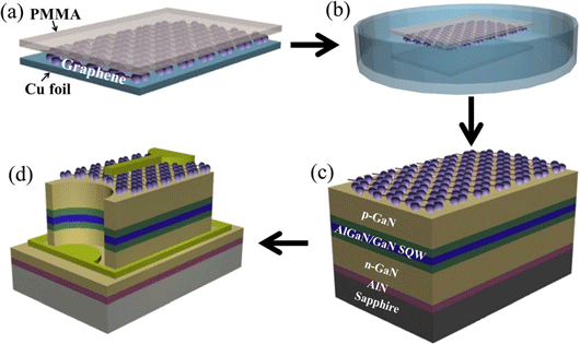
Figure 1: Schematic of the processes used to fabricate UV LED with a graphene-based transparent conductive electrode. FLG on the Cu foil was grown by CVD. (a) PMMA was coated on the graphene layer. (b) Cu foil on the graphene layer was removed by wet etching in ammonium persulfate. (c) Graphene with PMMA was deposited on p-GaN layer and PMMA was removed. (d) LED chips were fabricated by standard photolithographic processes.
The mesa structure of the LED was created after FLG transfer using a plasma etch of boron trichloride and chlorine gas (Figure 1d). The ohmic n-electrode consisted of 750°C annealed titanium-aluminum-nickel gold. Contact pads consisted of titanium-gold for both n- and p-type connections.
One advantage of using graphene over indium tin oxide (ITO) as transparent conductive oxide is its improved transmission in the ultraviolet. At 372nm, the transmittances of bi- (2L) and tetra-layer (4L) graphene were found to be 95% and 89%, respectively. By contrast, the value for 150nm ITO was 68%. This advantage for graphene lessens for longer wavelengths and disappears around 600nm.
The survival of the graphene layer from the LED process was confirmed by Raman spectroscopy, which also determined the number of layers by comparing the intensity of the peaks from the G and 2D bands arising from vibration/phonon modes.
The effect of using a 4L-graphene transparent contact was to double the injection current in LEDs: at 10V bias, an LED without graphene p-contact carried 2.3mA, and with the 4L-graphene carrying 5mA (Figure 2a). The main UV emission at 20mA occurs at 372nm (Figure 2b). The broad green-yellow (500–600nm) emission is attributed to “nitrogen vacancy and other growth related defects in the GaN”. Increased light output was also seen for 20mW input power (Figures 2c and d). Without graphene, light is only emitted from the edges of the structure. The 4L-graphene acts to spread the injection current and cause the whole device to emit.
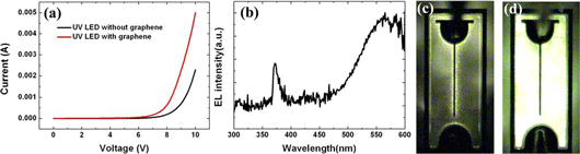
Figure 2: (a) The I–V characteristics of the UV LED with and without FLG-based transparent conductive electrode. (b) The EL spectra of UV LEDs. Optical images of light emission of UV LEDs (c) without and (d) with FLG-based transparent conductive electrode.
There is a trade-off between the conductivity of graphene and transparency. Thicker layers are more conductive, but transmit less UV.
The FLG contact LED could sustain 10mW input power for an “extended period of time”. However, increasing to 20mW reduced light output. The emission pattern that resulted was similar to that of the LED without FLG transparent conductive layer, suggesting that high-power operation removed the graphene layer. Raman spectroscopy investigation suggested that after a minute, the 4L layer had been reduced to 2L, which is less effective at spreading the injection current due to its lower conductivity.
The researchers conclude: “This study confirms that graphene-based transparent contact to a GaN-based UV LED is superior to an ITO contact based on cost, transparency, and, heat and current spreading. However, critical issues such as reliability and degradation of graphene films require and are the subject of further investigation.”
Funding for the research came from National Research Foundation of Korea (NRF), LG Innotek-Korea University Nano-Photonics Program, and the US Office of Naval Research.
The author Mike Cooke is a freelance technology journalist who has worked in the semiconductor and advanced technology sectors since 1997.