| Home | About Us | Contribute | Bookstore | Advertising | Subscribe for Free NOW! |
| News Archive | Features | Events | Recruitment | Directory |
News
26 May 2010
Fujitsu and University of Tokyo claim first 25Gb/s data transmission using QD laser
At last week's Conference on Lasers and Electro-Optics and the Quantum Electronics and Laser Science Conference (CLEO/QELC 2010) in San Jose, CA, USA (16-21 May), Japan's Fujitsu Ltd, Fujitsu Laboratories Ltd and the University of Tokyo presented what is claimed to be the first 25Gb/s high-speed data transmission using a quantum dot laser (which is expected to be the next generation of semiconductor laser capable of handling high-speed data transmissions while consuming minimal power).
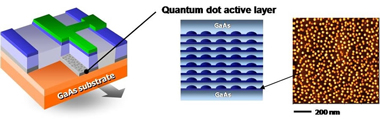
Picture: QD laser featuring an active layer containing high-density arrays of quantum dots.
QD lasers use quantum dots as the active lasing material. As increasing the number of quantum dots is known to improve the operating speed, layers of quantum dots with a higher density than normal were stacked, doubling the laser's operating speed and enabling a significant improvement over previous technologies. The technology is expected to be used in optical sources for next-generation high-speed data communications aiming to boost transmission speed tenfold to 100Gb/s.
Fujitsu and Fujitsu Laboratories have developed QD lasers in an industrial-academic collaboration with the laboratory of professor Yasuhiko Arakawa at the University of Tokyo. Advantages over other types of semiconductor laser include being less sensitive to temperature fluctuations, while offering lower power consumption, greater transmission distances, and faster speeds. There is hence much expectation that QD lasers will become core technology for developing high-performance optical sources in the future, to accommodate the rise in optical communications data traffic.
In accordance with the growth of broadband Internet bandwidths attributable to emerging services, such as cloud computing services and high-definition video download services, there has been rapid increase in such network traffic, says Fujitsu. To keep pace with data transmission volumes that continue to grow larger each year, optical networks need to run faster and be expanded to handle higher volumes of data.
Currently, 10Gb/s transmissions are the mainstream for data transmission. But, in view of transmission speeds rising continually, 100 Gigbit Ethernet (100GbE) - with data transmission speeds ten times as fast as currently available - is being promoted by the Institute of Electrical and Electronic Engineers (IEEE) as an international standard for next-generation high-speed datacoms. Accordingly, there is a need for laser light sources that can handle such next-generation high-speed data transmissions, while consuming only low power.
Quantum well lasers, conventionally used as optical sources for datacoms, have a problem of dramatic increases in power consumption due to increased driving current when temperatures rise. The QD laser developed by Fujitsu Laboratories and the University of Tokyo uses three-dimensional (3D) semiconductor nanostructures to produce quantum effects, giving it characteristics including stable operation over a range of temperatures as well as low power consumption. However, the QD laser had been limited to data transfer speeds up to 10Gb/s.
To increase the speed, it was necessary to increase the laser's optical gain, which in turn required an increase in the number of underlying quantum dots. New quantum dot fabrication technology was therefore developed and applied, resulting in a QD laser capable of operations at 25Gb/s.
The quantum dots are fabricated using molecular beam epitaxy to embed indium (In) and arsenide (As) in gallium arsenide. Because the atomic distance in indium arsenide (InAs) is greater than in GaAs, strain is induced in the InAs crystallized on the GaAs substrate. The strain energy can be relaxed by forming 3D crystals, in which each 3D nanocrystal functions as a single quantum dot.
By optimizing the growth conditions in which the 3D crystals are formed, the in-plane area density of the InAs quantum dots (the number of quantum dots per unit area) formed on the surface of the GaAs substrate has been doubled to 6 x 10¹⁰ per cm2.
Secondly, technology was developed that allows eight layers of quantum dots (up from five previously) to be stacked while preserving the same high-density in-plane (see Figure).
Using these fabrication techniques therefore enabled an increase in the total number of quantum dots in the active layer, increasing the optical gain. This hence allowed a QD laser to be tested operating at 25Gb/s modulation speed for the first time, Fujitsu claims.
The new technology makes it possible for temperature-stable, low-power-consumption QD lasers to be used for next-generation high-speed communications applications such as 100GbE, the firm reckons. It also obviates the need for expensive packages with embedded temperature controllers, helping to lower costs.
The new technology represents a step towards implementing QD lasers as an optical source for high-speed communications, says Fujitsu. Fujitsu Laboratories and the University of Tokyo plan to further refine the technology to increase the transmission distance and to confirm reliability. Tokyo-based QD Laser Inc, which was founded in 2006 with funding from Fujitsu Ltd and Mitsui Ventures, is also considering commercializing the technology.
Part of the research was carried out under a project contracted to the Photonics Electronics Technology Research Association (PETRA) by the New Energy and Industrial Technology Development Organization (NEDO), while part of the research was carried out under Japan's Ministry of Education, Culture, Sports, Science and Technology's Special Coordination Funds for Promoting Science and Technology.
![]() Search: Fujitsu Quantum dot laser InAs quantum dots GaAs substrate
Search: Fujitsu Quantum dot laser InAs quantum dots GaAs substrate
Visit: http://jp.fujitsu.com/labs/en
Visit: www.u-tokyo.ac.jp
![]() ©2010 Juno Publishing and Media Solutions Ltd. All rights reserved. Semiconductor Today and the editorial material contained within it and related media is the copyright of Juno Publishing and Media Solutions Ltd. Reproduction in whole or part without permission from Juno Publishing and Media Solutions Ltd is forbidden. In most cases, permission will be granted, if the author, magazine and publisher are acknowledged.
©2010 Juno Publishing and Media Solutions Ltd. All rights reserved. Semiconductor Today and the editorial material contained within it and related media is the copyright of Juno Publishing and Media Solutions Ltd. Reproduction in whole or part without permission from Juno Publishing and Media Solutions Ltd is forbidden. In most cases, permission will be granted, if the author, magazine and publisher are acknowledged.
Disclaimer: Material published within Semiconductor Today and related media does not necessarily reflect the views of the publisher or staff. Juno Publishing and Media Solutions Ltd and its staff accept no responsibility for opinions expressed, editorial errors and damage/injury to property or persons as a result of material published.
Semiconductor Today, Juno Publishing and Media Solutions Ltd, Suite no. 133, 20 Winchcombe Street, Cheltenham, GL52 2LY, UK
Web site by No Name No Slogan ![]()